SNLS302E May 2010 – February 2015 DS92LV2411 , DS92LV2412
PRODUCTION DATA.
- 1 Features
- 2 Applications
- 3 Description
- 4 Revision History
- 5 Pin Configuration and Functions
-
6 Specifications
- 6.1 Absolute Maximum Ratings
- 6.2 ESD Ratings
- 6.3 Recommended Operating Conditions
- 6.4 Thermal Information
- 6.5 Serializer DC Electrical Characteristics
- 6.6 Deserializer DC Electrical Characteristics
- 6.7 DC and AC Serial Control Bus Characteristics
- 6.8 Recommended Timing For The Serial Control Bus
- 6.9 Recommended Serializer Timing For CLKIN
- 6.10 Serializer Switching Characteristics
- 6.11 Deserializer Switching Characteristics
- 6.12 Typical Characteristics
-
7 Detailed Description
- 7.1 Overview
- 7.2 Functional Block Diagrams
- 7.3
Feature Description
- 7.3.1 Serializer Functional Description
- 7.3.2
Deserializer Functional Description
- 7.3.2.1 Integrated Signal Conditioning Features — Des
- 7.3.2.2 EMI Reduction Features
- 7.3.2.3 Power Saving Features
- 7.3.2.4 Des — Clock-Data Recovery Status Flag (Lock) And Output State Select (OSS_SEL)
- 7.3.2.5 Des — Oscillator Output — Optional
- 7.3.2.6 Des — OP_LOW — Optional
- 7.3.2.7 Des — Clock Edge Select (RFB)
- 7.3.2.8 Des — Control Signal Filter — Optional
- 7.3.2.9 Des — SSCG Low Frequency Optimization (Lf_mode)
- 7.3.2.10 Des — Strap Input Pins
- 7.3.3 Built In Self Test (BIST)
- 7.4 Device Functional Modes
- 7.5 Programming
- 7.6 Register Maps
- 8 Applications and Implementation
- 9 Power Supply Recommendations
- 10Layout
- 11Device and Documentation Support
- 12Mechanical, Packaging, and Orderable Information
5 Pin Configuration and Functions
48-Pin WQFN
Package RHS
Top View
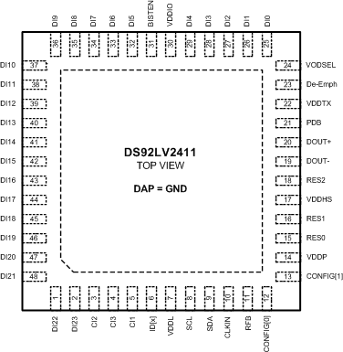
Pin Functions, DS92LV2411 Serializer(1)
| PIN | TYPE | DESCRIPTION | |
|---|---|---|---|
| NAME | NO. | ||
| LVCMOS PARALLEL INTERFACE | |||
| CI1 | 5 | I, LVCMOS w/ pull-down |
Control Signal Input For Display/Video Application: CI1 = Data Enable Input Control signal pulse width must be 3 clocks or longer to be transmitted when the Control Signal Filter is enabled (CONFIG[1:0] = 01). There is no restriction on the minimum transition pulse when the Control Signal Filter is disabled (CONFIG[1:0] = 00). The signal is limited to 2 transitions per 130 clocks regardless of the Control Signal Filter setting. |
| CI2 | 3 | I, LVCMOS w/ pull-down |
Control Signal Input For Display/Video Application: CI2 = Horizontal Sync Input Control signal pulse width must be 3 clocks or longer to be transmitted when the Control Signal Filter is enabled (CONFIG[1:0] = 01). There is no restriction on the minimum transition pulse when the Control Signal Filter is disabled (CONFIG[1:0] = 00). The signal is limited to 2 transitions per 130 clocks regardless of the Control Signal Filter setting. |
| CI3 | 4 | I, LVCMOS w/ pull-down |
Control Signal Input For Display/Video Application: CI3 = Vertical Sync Input CI3 is limited to 1 transition per 130 clock cycles. Thus, the minimum pulse width allowed is 130 clock cycle wide. |
| CLKIN | 10 | I, LVCMOS w/ pull-down |
Clock Input Latch/data strobe edge set by RFB Pin. |
| DI[7:0] | 34, 33, 32, 29, 28, 27, 26, 25 | I, LVCMOS w/ pull-down |
Parallel Interface Data Input Pins For 8–bit RED Display: DI7 = R7 – MSB, DI0 = R0 – LSB. |
| DI[15:8] | 42, 41, 40, 39, 38, 37, 36, 35 | I, LVCMOS w/ pull-down |
Parallel Interface Data Input Pins For 8–bit GREEN Display: DI15 = G7 – MSB, DI8 = G0 – LSB. |
| DI[23:16] | 2, 1, 48, 47, 46, 45, 44, 43 | I, LVCMOS w/ pull-down |
Parallel Interface Data Input Pins For 8–bit BLUE Display: DI23 = B7 – MSB, DI16 = B0 – LSB. |
| CONTROL AND CONFIGURATION | |||
| BISTEN | 31 | I, LVCMOS w/ pull-down |
BIST Mode — Optional BISTEN = 0, BIST is disabled (normal operation) BISTEN = 1, BIST is enabled |
| CONFIG[1:0] | 13, 12 | I, LVCMOS w/ pull-down |
00: Control Signal Filter DISABLED. Interfaces with DS92LV2412 or DS92LV0412 01: Control Signal Filter ENABLED. Interfaces with DS92LV2412 or DS92LV0412 10: Reverse compatibility mode to interface with the DS90UR124 or DS99R124Q 11: Reverse compatibility mode to interface with the DS90C124 |
| De-Emph | 23 | I, Analog w/ pull-up |
De-Emphasis Control De-Emph = open (float) - disabled To enable De-emphasis, tie a resistor from this Pin to GND or control via register. See Table 2. This can also be controlled by I2C register access. |
| ID[x] | 6 | I, Analog | I2C Serial Control Bus Device ID Address Select — Optional Resistor to Ground and 10 kΩ pull-up to 1.8V rail. See Table 11. |
| PDB | 21 | I, LVCMOS w/ pull-down |
Power-down Mode Input PDB = 1, Ser is enabled (normal operation). Refer to ”Power Up Requirements and PDB Pin” in the Applications Information Section. PDB = 0, Ser is powered down When the Ser is in the power-down state, the driver outputs (DOUT+/-) are both logic high, the PLL is shutdown, IDD is minimized. Control Registers are RESET. |
| RES[2:0] | 18, 16, 15 | I, LVCMOS w/ pull-down |
Reserved - tie LOW |
| RFB | 11 | I, LVCMOS w/ pull-down |
Clock Input Latch/Data Strobe Edge Select RFB = 1, parallel interface data and control signals are latched on the rising clock edge. RFB = 0, parallel interface data and control signals are latched on the falling clock edge. This can also be controlled by I2C register access. |
| SCL | 8 | I, LVCMOS Open Drain |
I2C Serial Control Bus Clock Input - Optional SCL requires an external pull-up resistor to 3.3V. |
| SDA | 9 | I/O, LVCMOS Open Drain |
I2C Serial Control Bus Data Input / Output - Optional SDA requires an external pull-up resistor 3.3V. |
| VODSEL | 24 | I, LVCMOS w/ pull-down |
Differential Driver Output Voltage Select VODSEL = 1, CML VOD is ±420 mV, 840 mVp-p (typ) — long cable / De-Emph applications VODSEL = 0, CML VOD is ±280 mV, 560 mVp-p (typ) — short cable (no De-emph), low power mode. This is can also be control by I2C register. |
| CHANNEL-LINK II — CML SERIAL INTERFACE | |||
| DOUT- | 19 | O, CML | Inverting Output. The output must be AC Coupled with a 0.1 µF capacitor. |
| DOUT+ | 20 | O, CML | Non–Inverting Output. The output must be AC Coupled with a 0.1 µF capacitor. |
| POWER AND GROUND | |||
| GND | DAP | Ground | DAP is the large metal contact at the bottom side, located at the center of the WQFN package. Connect to the ground plane (GND) with at least 9 vias. |
| VDDHS | 17 | Power | TX High Speed Logic Power, 1.8 V ±5% |
| VDDIO | 30 | Power | LVCMOS I/O Power, 1.8 V ±5% OR 3.3 V ±10% |
| VDDL | 7 | Power | Logic Power, 1.8 V ±5% |
| VDDP | 14 | Power | PLL Power, 1.8 V ±5% |
| VDDTX | 22 | Power | Output Driver Power, 1.8 V ±5% |
(1) NOTE: 1 = HIGH, 0 = LOW
The VDD (VDDn and VDDIO) supply ramp should be faster than 1.5 ms with a monotonic rise. If slower then 1.5 ms then a capacitor on the PDB Pin is needed to ensure PDB arrives after all the VDD have settled to the recommended operating voltage.
The VDD (VDDn and VDDIO) supply ramp should be faster than 1.5 ms with a monotonic rise. If slower then 1.5 ms then a capacitor on the PDB Pin is needed to ensure PDB arrives after all the VDD have settled to the recommended operating voltage.
60-Pin WQFN
Package NKB
Top View
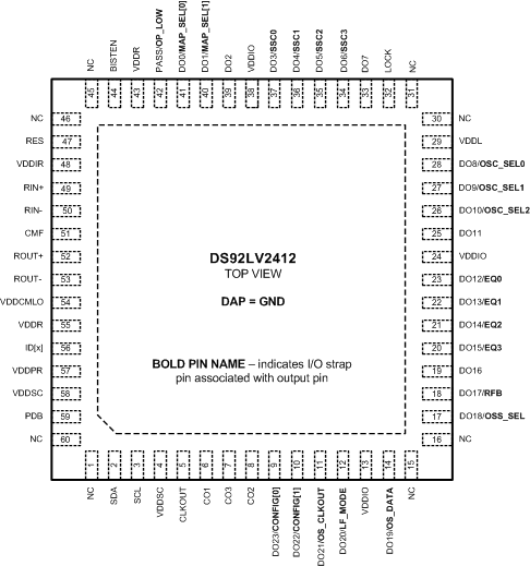
Pin Functions, DS92LV2412 Deserializer (1)
| PIN | TYPE | DESCRIPTION | |
|---|---|---|---|
| NAME | NO. | ||
| LVCMOS PARALLEL INTERFACE | |||
| CLKOUT | 5 | O, LVCMOS | Pixel Clock Output In power-down (PDB = 0), output is controlled by the OSS_SEL Pin (See Table 6). Data strobe edge set by RFB. |
| CO1 | 6 | O, LVCMOS | Control Signal Output For Display/Video Application: CO1 = Data Enable Output Control signal pulse width must be 3 clocks or longer to be transmitted when the Control Signal Filter is enabled (CONFIG[1:0] = 01). There is no restriction on the minimum transition pulse when the Control Signal Filter is disabled (CONFIG[1:0] = 00). The signal is limited to 2 transitions per 130 clocks regardless of the Control Signal Filter setting. In power-down (PDB = 0), output is controlled by the OSS_SEL Pin (See Table 6). |
| CO2 | 8 | O, LVCMOS | Control Signal Output For Display/Video Application: CO2 = Horizontal Sync Output Control signal pulse width must be 3 clocks or longer to be transmitted when the Control Signal Filter is enabled (CONFIG[1:0] = 01). There is no restriction on the minimum transition pulse when the Control Signal Filter is disabled (CONFIG[1:0] = 00). The signal is limited to 2 transitions per 130 clocks regardless of the Control Signal Filter setting. In power-down (PDB = 0), output is controlled by the OSS_SEL Pin (See Table 6). |
| CO3 | 7 | O, LVCMOS | Control Signal Output For Display/Video Application: CO3 = Vertical Sync Output CO3 is different than CO1 and CO2 because it is limited to 1 transition per 130 clock cycles. Thus, the minimum pulse width allowed is 130 clock cycle wide. The CONFIG[1:0] Pins have no affect on CO3 signal In power-down (PDB = 0), output is controlled by the OSS_SEL Pin (See Table 6). |
| DO[7:0] | 33, 34, 35, 36, 37, 39, 40, 41 | I, STRAP, O, LVCMOS |
Parallel Interface Data Output Pins For 8–bit RED Display: DO7 = R7 – MSB, DO0 = R0 – LSB. In power-down (PDB = 0), outputs are controlled by the OSS_SEL (See Table 6). These Pins are inputs during power-up (See STRAP Inputs). |
| DO[15:8] | 20, 21, 22, 23, 25, 26, 27, 28 | I, STRAP, O, LVCMOS |
Parallel Interface Data Output Pins For 8–bit GREEN Display: DO15 = G7 – MSB, DO8 = G0 – LSB. In power-down (PDB = 0), outputs are controlled by the OSS_SEL (See Table 6). These Pins are inputs during power-up (See STRAP Inputs). |
| DO[23:16] | 9, 10, 11, 12, 14, 17, 18, 19 | I, STRAP, O, LVCMOS |
Parallel Interface Data Input Pins For 8–bit BLUE Display: DO23 = B7 – MSB, DO16 = B0 – LSB. In power-down (PDB = 0), outputs are controlled by the OSS_SEL (See Table 6). These Pins are inputs during power-up (See STRAP Inputs). |
| LOCK | 32 | O, LVCMOS | LOCK Status Output LOCK = 1, PLL is Locked, outputs are active LOCK = 0, PLL is unlocked, DO[23:0], CO1, CO2, CO3 and CLKOUT output states are controlled by OSS_SEL (See Table 6). May be used as Link Status or to flag when Video Data is active (ON/OFF). |
| PASS | 42 | O, LVCMOS | PASS Output (BIST Mode) PASS = 1, error free transmission PASS = 0, one or more errors were detected in the received payload Route to test point for monitoring, or leave open if unused. |
| CONTROL AND CONFIGURATION — STRAP PINS (2) | |||
| CONFIG[1:0] | 10 [DO22], 9 [DO23] |
STRAP I, LVCMOS w/ pull-down |
00: Control Signal Filter DISABLED. Interfaces with DS92LV2411 or DS92LV0411 01: Control Signal Filter ENABLED. Interfaces with DS92LV2411 or DS92LV0411 10: Reverse compatibility mode to interface with the DS90UR241 or DS99R241 11: Reverse compatibility mode to interface with the DS90C241 |
| EQ[3:0] | 20 [DO15], 21 [DO14], 22 [DO13], 23 [DO12] |
STRAP I, LVCMOS w/ pull-down |
Receiver Input Equalization (See Table 3). This can also be controlled by I2C register access. |
| LF_MODE | 12 [DO20] | STRAP I, LVCMOS w/ pull-down |
SSCG Low Frequency Mode Only required when SSCG is enabled, otherwise LF_MODE condition is a DON’T CARE (X). LF_MODE = 1, SSCG in low frequency mode (CLK = 5-20 MHz) LF_MODE = 0, SSCG in high frequency mode (CLK = 20-50 MHz) This can also be controlled by I2C register access. |
| MAP_SEL[1:0] | 40[D], 41 [D] |
STRAP I, LVCMOS w/ pull-down |
Bit mapping reverse compatibility / DS90UR241 Options Pin or Register Control Default setting is b'00. |
| OP_LOW | 42 [PASS] | STRAP I, LVCMOS w/ pull-down |
Outputs held LOW when LOCK = 1 NOTE: Do not use any other strap options with this strap function enabled OP_LOW = 1: all outputs are held LOW during power up until released by programming OP_LOW release/set register HIGH. NOTE: Before the device is powered up, the outputs are in TRI-STATE See Figure 26 and Figure 27 OP_LOW = 0: all outputs toggle normally as soon as LOCK goes HIGH (default) This can also be controlled by I2C register access. |
| OS_CLKOUT | 11 [DO21] | STRAP I, LVCMOS w/ pull-down |
Output CLKOUT Slew Select OS_CLKOUT = 1, Increased CLKOUT slew rate OS_CLKOUT = 0, Normal CLKOUT slew rate (default) This can also be controlled by I2C register access. |
| OS_DATA | 14 [DO19] | STRAP I, LVCMOS w/ pull-down |
Output DO[23:0], CO1, CO2, CO3 Slew Select OS_DATA = 1, Increased DO slew rate OS_DATA = 0, Normal DO slew rate (default) This can also be controlled by I2C register access. |
| OSS_SEL | 17 [DO18] | STRAP I, LVCMOS w/ pull-down |
Output Sleep State Select OSS_SEL is used in conjunction with PDB to determine the state of the outputs in Power Down (Sleep). (See Table 6). NOTE: OSS_SEL STRAP CANNOT BE USED IF OP_LOW = 1 This can also be controlled by I2C register access. |
| RFB | 18 [DO17] | STRAP I, LVCMOS w/ pull-down |
Clock Output Strobe Edge Select RFB = 1, parallel interface data and control signals are strobed on the rising clock edge. RFB = 0, parallel interface data and control signals are strobed on the falling clock edge. This can also be controlled by I2C register access. |
| OSC_SEL[2:0] | 26 [DO10], 27 [DO9], 28 [DO8] |
STRAP I, LVCMOS w/ pull-down |
Oscillator Selectl (See Table 7 and Table 8). This can also be controlled by I2C register access. |
| SSC[3:0] | 34 [DO6], 35 [DO5], 36 [DO4], 37 [DO3] |
STRAP I, LVCMOS w/ pull-down |
Spread Spectrum Clock Generation (SSCG) Range Select (See Table 4 and Table 5). This can also be controlled by I2C register access. |
| CONTROL AND CONFIGURATION | |||
| BISTEN | 44 | I, LVCMOS w/ pull-down |
BIST Enable Input — Optional BISTEN = 0, BIST is disabled (normal operation) BISTEN = 1, BIST is enabled |
| ID[x] | 56 | I, Analog | I2C Serial Control Bus Device ID Address Select — Optional Resistor to Ground and 10 kΩ pull-up to 1.8V rail. (See Table 11). |
| NC | 1, 15, 16, 30, 31, 45, 46, 60 | Not Connected Leave Pin open (float) |
|
| PDB | 59 | I, LVCMOS w/ pull-down |
Power Down Mode Input PDB = 1, Des is enabled (normal operation). Refer to “Power Up Requirements and PDB Pin” in the Applications Information Section. PDB = 0, Des is in power-down. When the Des is in the power-down state, the LVCMOS output state is determined by Table 6. Control Registers are RESET. |
| RES | 47 | I, LVCMOS w/ pull-down |
Reserved - tie LOW |
| SCL | 3 | I, LVCMOS Open Drain |
I2C Serial Control Bus Clock Input - Optional SCL requires an external pull-up resistor to 3.3V. |
| SDA | 2 | I/O, LVCMOS Open Drain |
I2C Serial Control Bus Data Input / Output - Optional SDA requires an external pull-up resistor to 3.3V. |
| CHANNEL-LINK II — CML SERIAL INTERFACE | |||
| CMF | 51 | I, Analog | Common-Mode Filter VCM center-tap is a virtual ground which may be AC coupled to ground to increase receiver common mode noise immunity. Recommended value is 4.7 μF or higher. |
| RIN+ | 49 | I, CML | True Input. The input must be AC Coupled with a 0.1 μF capacitor. |
| RIN- | 50 | I, CML | Inverting Input. The input must be AC Coupled with a 0.1 μF capacitor. |
| ROUT+ | 52 | O, CML | True Output — Receive Signal after the Equalizer NC if not used or connect to test point for monitor. Requires I2C control to enable. |
| ROUT- | 53 | O, CML | Inverting Output — Receive Signal after the Equalizer NC if not used or connect to test point for monitor. Requires I2C control to enable. |
| POWER AND GROUND(3) | |||
| GND | DAP | Ground | DAP is the large metal contact at the bottom side, located at the center of the WQFN package. Connected to the ground plane (GND) with at least 9 vias. |
| VDDCMLO | 54 | Power | RX High Speed Logic Power, 1.8 V ± 5% |
| VDDIO | 13, 24, 38 | Power | LVCMOS I/O Power, 1.8 V ± 5% OR 3.3 V ± 10% (VDDIO) |
| VDDIR | 48 | Power | Input Power, 1.8 V ±5% |
| VDDL | 29 | Power | Logic Power, 1.8 V ±5% |
| VDDPR | 57 | Power | PLL Power, 1.8 V ±5% |
| VDDR | 43, 55 | Power | RX High Speed Logic Power, 1.8 V ±5% |
| VDDSC | 4, 58 | Power | SSCG Power, 1.8 V ±5% |
(1) NOTE: 1 = HIGH, 0 = LOW
The VDD (VDDn and VDDIO) supply ramp should be faster than 1.5 ms with a monotonic rise. If slower then 1.5 ms then a capacitor on the PDB Pin is needed to ensure PDB arrives after all the VDD have settled to the recommended operating voltage.
The VDD (VDDn and VDDIO) supply ramp should be faster than 1.5 ms with a monotonic rise. If slower then 1.5 ms then a capacitor on the PDB Pin is needed to ensure PDB arrives after all the VDD have settled to the recommended operating voltage.
(2) For a High State, use a 10 kΩ pull up to VDDIO; for a Low State, the IO includes an internal pull down. The STRAP Pins are read upon power-up and set device configuration. Pin Number listed along with shared data output name in square brackets.
(3) Power must be supplied to all power Pins for normal operation