JAJSPC0 November   2022 ESD2CANFD24

PRODUCTION DATA  

  1. 特長
  2. アプリケーション
  3. 概要
  4. Revision History
  5. Pin Configuration and Functions
  6. Specifications
    1. 6.1 絶対最大定格
    2. 6.2 ESD 定格 - JEDEC 仕様
    3. 6.3 ESD 定格 - IEC 仕様
    4. 6.4 推奨動作条件
    5. 6.5 熱に関する情報
    6. 6.6 電気的特性
    7. 6.7 Typical Characteristics – ESD2CANFD24
  7. Detailed Description
    1. 7.1 Overview
    2. 7.2 Functional Block Diagram
    3. 7.3 Feature Description
      1. 7.3.1 Temperature Range
      2. 7.3.2 IEC 61000-4-2 ESD Protection
      3. 7.3.3 IEC 61000-4-5 Surge Protection
      4. 7.3.4 IO Capacitance
      5. 7.3.5 Dynamic Resistance
      6. 7.3.6 DC Breakdown Voltage
      7. 7.3.7 Ultra Low Leakage Current
      8. 7.3.8 Clamping Voltage
      9. 7.3.9 Industry Standard Leaded Packages
    4. 7.4 Device Functional Modes
  8. Application and Implementation
    1. 8.1 Application Information
    2. 8.2 Typical Application
      1. 8.2.1 Design Requirements
      2. 8.2.2 Detailed Design Procedure
      3. 8.2.3 Application Curves
  9. Power Supply Recommendations
  10. 10Layout
    1. 10.1 Layout Guidelines
    2. 10.2 Layout Example
  11. 11Device and Documentation Support
    1. 11.1 Documentation Support
      1. 11.1.1 Related Documentation
    2. 11.2 Receiving Notification of Documentation Updates
    3. 11.3 サポート・リソース
    4. 11.4 Trademarks
    5. 11.5 Electrostatic Discharge Caution
    6. 11.6 Glossary
  12. 12Mechanical, Packaging, and Orderable Information

パッケージ・オプション

メカニカル・データ(パッケージ|ピン)
サーマルパッド・メカニカル・データ
発注情報

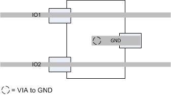
Layout Example

This example is typical of a dual channel differential data pair application, such as CAN.
GUID-A82B79E8-C597-418D-A9CC-FD15ADDA3A25-low.gifFigure 10-1 Routing with DBZ Package