SLAS840C March 2012 – October 2015 HD3SS3415
PRODUCTION DATA.
- 1 Features
- 2 Applications
- 3 Description
- 4 Revision History
- 5 Description continued
- 6 Pin Configuration and Functions
- 7 Specifications
- 8 Parameter Measurement Information
- 9 Detailed Description
- 10Application and Implementation
- 11Power Supply Recommendations
- 12Layout
- 13Device and Documentation Support
- 14Mechanical, Packaging, and Orderable Information
パッケージ・オプション
メカニカル・データ(パッケージ|ピン)
- RUA|42
サーマルパッド・メカニカル・データ
- RUA|42
発注情報
12 Layout
12.1 Layout Guidelines
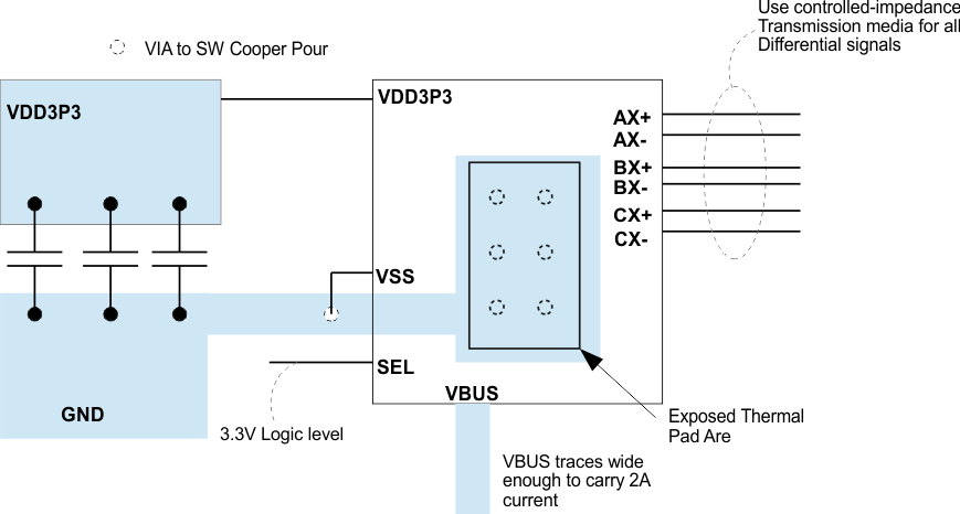
- Decoupling caps should be placed next to each power terminal on the HD3SS3415. Take care to minimize the stub length of the trace connecting the capacitor to the power pin.
- Avoid sharing vias between multiple decoupling caps.
- Place vias as close as possible to the decoupling cap solder pad.
- Widen VDD/GND planes to reduce effect of static and dynamic IR drop.
- The VBUS traces/planes must be wide enough to carry maximum of 2 A current
12.2 Layout Example
 Figure 17. Layout Example