JAJSF23B March   2018  – July 2018 INA1620

PRODUCTION DATA.  

  1. 特長
  2. アプリケーション
  3. 概要
    1.     Device Images
      1.      INA1620の簡略化された内部回路図
      2.      FFT: 1kHz、32Ω負荷、50mW
  4. 改訂履歴
  5. Pin Configuration and Functions
    1.     Pin Functions
  6. Specifications
    1. 6.1 Absolute Maximum Ratings
    2. 6.2 ESD Ratings
    3. 6.3 Recommended Operating Conditions
    4. 6.4 Thermal Information
    5. 6.5 Electrical Characteristics:
    6. 6.6 Typical Characteristics
  7. Detailed Description
    1. 7.1 Overview
    2. 7.2 Functional Block Diagram
    3. 7.3 Feature Description
      1. 7.3.1 Matched Thin-Film Resistor Pairs
      2. 7.3.2 Power Dissipation
      3. 7.3.3 Thermal Shutdown
      4. 7.3.4 EN Pin
      5. 7.3.5 GND Pin
      6. 7.3.6 Input Protection
    4. 7.4 Device Functional Modes
      1. 7.4.1 Shutdown Mode
      2. 7.4.2 Output Transients During Power Up and Power Down
  8. Application and Implementation
    1. 8.1 Application Information
      1. 8.1.1 Noise Performance
      2. 8.1.2 Resistor Tolerance
      3. 8.1.3 EMI Rejection
      4. 8.1.4 EMIRR +IN Test Configuration
    2. 8.2 Typical Application
      1. 8.2.1 Design Requirements
      2. 8.2.2 Detailed Design Procedure
      3. 8.2.3 Application Curves
    3. 8.3 Other Application Examples
      1. 8.3.1 Preamplifier for Professional Microphones
  9. Power Supply Recommendations
  10. 10Layout
    1. 10.1 Layout Guidelines
    2. 10.2 Layout Example
  11. 11デバイスおよびドキュメントのサポート
    1. 11.1 デバイス・サポート
      1. 11.1.1 開発サポート
        1. 11.1.1.1 TINA-TI(無料のダウンロード・ソフトウェア)
        2. 11.1.1.2 TI Precision Designs
    2. 11.2 ドキュメントのサポート
      1. 11.2.1 関連資料
    3. 11.3 ドキュメントの更新通知を受け取る方法
    4. 11.4 コミュニティ・リソース
    5. 11.5 商標
    6. 11.6 静電気放電に関する注意事項
    7. 11.7 Glossary
  12. 12メカニカル、パッケージ、および注文情報

パッケージ・オプション

メカニカル・データ(パッケージ|ピン)
サーマルパッド・メカニカル・データ
発注情報

Output Transients During Power Up and Power Down

To minimize the possibility of output transients that might produce an audible click or pop, ramp the supply voltages for the INA1620 symmetrically to their nominal values. Asymmetrical supply ramping can cause output transients during power up that can be audible in headphone applications. If possible, hold the EN pin low while the power supplies are ramping up or down. If the EN pin is not being independently controlled (for example, by a GPIO pin), use a voltage divider to hold the enable pin voltage below the logic-high threshold until the power supplies reach the specified minimum voltage, as shown in Figure 50.
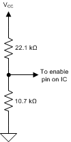
INA1620 d306_enablevdiv_u.gifFigure 50. Voltage Divider Used to Hold Enable Low at Power-Up or Power-Down