JAJSCS8B December 2016 – November 2018 INA1650 , INA1651
PRODUCTION DATA.
- 1 特長
- 2 アプリケーション
- 3 概要
- 4 改訂履歴
- 5 Pin Configuration and Functions
- 6 Specifications
- 7 Detailed Description
-
8 Application and Implementation
- 8.1 Application Information
- 8.2
Typical Applications
- 8.2.1 Line Receiver for Differential Audio Signals in a Split-Supply System
- 8.2.2 Differential Line Receiver for Single-Supply Applications
- 8.2.3 Floating Single-Ended Input Line Receiver for Ground Loop Noise Reduction
- 8.2.4 Floating Single-Ended Input Line Receiver With Differential Outputs
- 8.2.5 TRS Audio Interface in Single-Supply Applications
- 8.2.6 Differential Line Driver With Single-Ended Input
- 9 Power Supply Recommendations
- 10Layout
- 11デバイスおよびドキュメントのサポート
- 12メカニカル、パッケージ、および注文情報
8.2.6 Differential Line Driver With Single-Ended Input
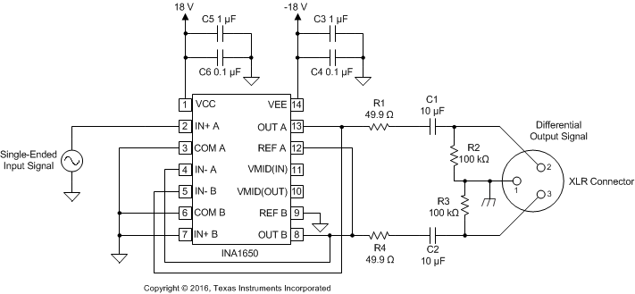
The INA1650 can be employed in line-driver applications (Figure 62) where the precision matched internal resistor networks are useful in converting a single-ended signal to a balanced signal. Resistors R1 and R4 (shown in Figure 62) isolate the large cable capacitance from the outputs of the INA1650 to maintain stability. TI recommends AC-coupling capacitors C1 and C2 since the DC voltages of the connected equipment may be unknown. Resistors R2 and R3 dissipate any charge collected on the capacitors due to connecting equipment with a DC voltage present.
 Figure 62. INA1650 Used as a Balanced Audio Line Driver