JAJSL62 February   2021 INA183

PRODUCTION DATA  

  1. 特長
  2. アプリケーション
  3. 概要
  4. Revision History
  5. Device Comparison
  6. Pin Configuration and Functions
  7. Specifications
    1. 7.1 Absolute Maximum Ratings
    2. 7.2 ESD Ratings
    3. 7.3 Recommended Operating Conditions
    4. 7.4 Thermal Information
    5. 7.5 Electrical Characteristics
    6. 7.6 Typical Characteristics
  8. Detailed Description
    1. 8.1 Overview
    2. 8.2 Functional Block Diagram
    3. 8.3 Feature Description
      1. 8.3.1 Single-Supply Operation from IN+
      2. 8.3.2 Low Gain Error and Offset Voltage
      3. 8.3.3 Low Drift Architecture
    4. 8.4 Device Functional Modes
      1. 8.4.1 Normal Operation
      2. 8.4.2 Unidirectional, High-Side Operation
      3. 8.4.3 Input Differential Overload
  9. Application and Implementation
    1. 9.1 Application Information
      1. 9.1.1 RSENSE and Device Gain Selection
    2. 9.2 Typical Application
      1. 9.2.1 Design Requirements
      2. 9.2.2 Detailed Design Procedure
      3. 9.2.3 Application Curve
  10. 10Power Supply Recommendations
  11. 11Layout
    1. 11.1 Layout Guidelines
    2. 11.2 Layout Example
  12. 12Device and Documentation Support
    1. 12.1 Documentation Support
      1. 12.1.1 Related Documentation
    2. 12.2 ドキュメントの更新通知を受け取る方法
    3. 12.3 サポート・リソース
    4. 12.4 Trademarks
    5. 12.5 静電気放電に関する注意事項
    6. 12.6 用語集
  13. 13Mechanical, Packaging, and Orderable Information

パッケージ・オプション

メカニカル・データ(パッケージ|ピン)
サーマルパッド・メカニカル・データ
発注情報

Detailed Design Procedure

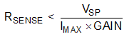
The maximum value of the current-sense resistor is calculated based on choice of gain, the value of the maximum current the be sensed (IMAX), and the power-supply voltage (VIN+). When operating at the maximum current, the output voltage must not exceed the positive output swing specification, VSP. Under the given design parameters, Equation 4 calculates the maximum value for RSENSE as 47.2 mΩ.

Equation 4. GUID-20200713-CA0I-RB5N-0HJ8-JNH9DN6GVL6K-low.gif

For this design example, a value of 40.2 mΩ is selected because, while the 40.2 mΩ is less than the maximum value calculated, 40.2 mΩ is still large enough to give an adequate signal at the current-sense amplifier output. To reduce resistor power losses or to operate over a reduced output range, smaller value resistors can be used as the expense of dynamic range and low current accuracy.