JAJSH29A March 2019 – November 2023 INA185
PRODUCTION DATA
- 1
- 1 特長
- 2 アプリケーション
- 3 概要
- 4 Pin Configuration and Functions
- 5 Specifications
- 6 Detailed Description
- 7 Application and Implementation
- 8 Device and Documentation Support
- 9 Revision History
- 10Mechanical, Packaging, and Orderable Information
パッケージ・オプション
メカニカル・データ(パッケージ|ピン)
サーマルパッド・メカニカル・データ
発注情報
7.2.2 Detailed Design Procedure
The maximum value of the current sense resistor is calculated based on the maximum power loss requirement. By applying Equation 2, the maximum value of the current-sense resistor is 1.125 mΩ. This is the maximum value for sense resistor RSENSE; therefore, set RSENSE to 1 mΩ as this value is the closest standard resistor value that meets the power-loss requirement.
The next step is to select the appropriate gain and reduce RSENSE, if needed, to keep the output signal swing within the VS range. The design requirements call for bidirectional current monitoring; therefore, a voltage between 0 and VS must be applied to the REF pin. The bidirectional currents monitored are symmetric around 0 (that is, ±20 A); therefore, the ideal voltage to apply to VREF is VS / 2 or 2.5 V. If the positive current is greater than the negative current, using a lower voltage on VREF has the benefit of maximizing the output swing for the given range of expected currents. Using Equation 3, and given that IMAX = 20 A , RSENSE = 1 mΩ, and VREF = 2.5 V, the maximum current-sense gain calculated to avoid the positive swing-to-rail limitations on the output is 122.5 V/V. Likewise, using Equation 4 for the negative-swing limitation results in a maximum gain of 124.75 V/V. Selecting the gain-of-100 device maximizes the output range while staying within the output swing range. If the maximum calculated gains are slightly less than 100 V/V, the value of the current-sense resistor can be reduced to keep the output from hitting the output-swing limitations.
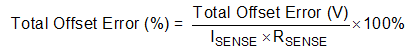
To calculate the accuracy at peak current, the two factors that must be determined are the gain error and the offset error. The gain error of the INA185A3 is specified to be a maximum of 0.2%. The error due to the offset is constant, and is specified to be 130 µV (maximum) for the conditions where VCM = 12 V and VS = 5 V. Using Equation 7, the percentage error contribution of the offset voltage is calculated to be 0.65%, with total offset error = 130 µV, RSENSE = 1 mΩ, and ISENSE = 20 A.
One method of calculating the total error is to add the gain error to the percentage contribution of the offset error. However, in this case, the gain error and the offset error do not have an influence or correlation to each other. A more statistically-accurate method of calculating the total error is to use the RSS sum of the errors, as shown in Equation 8:

After applying Equation 8, the total current sense error at maximum current is calculated to be 0.68%, which is less than the design example requirement of 1%.
The INA185A3 (gain = 100 V/V) also has a bandwidth of 150 kHz that meets the small-signal bandwidth requirement of 100 kHz. If higher bandwidth is required, lower-gain devices can be used at the expense of either reduced output voltage range or an increased value of RSENSE.