JAJSHG8B May   2019  – March 2022 INA186-Q1

PRODUCTION DATA  

  1. 特長
  2. アプリケーション
  3. 概要
  4. Revision History
  5. Pin Configuration and Functions
  6. Specifications
    1. 6.1 Absolute Maximum Ratings
    2. 6.2 ESD Ratings
    3. 6.3 Recommended Operating Conditions
    4. 6.4 Thermal Information
    5. 6.5 Electrical Characteristics
    6. 6.6 Typical Characteristics
  7. Detailed Description
    1. 7.1 Overview
    2. 7.2 Functional Block Diagram
    3. 7.3 Feature Description
      1. 7.3.1 Precision Current Measurement
      2. 7.3.2 Low Input Bias Current
      3. 7.3.3 Low Quiescent Current With Output Enable
      4. 7.3.4 Bidirectional Current Monitoring
      5. 7.3.5 High-Side and Low-Side Current Sensing
      6. 7.3.6 High Common-Mode Rejection
      7. 7.3.7 Rail-to-Rail Output Swing
    4. 7.4 Device Functional Modes
      1. 7.4.1 Normal Operation
      2. 7.4.2 Unidirectional Mode
      3. 7.4.3 Bidirectional Mode
      4. 7.4.4 Input Differential Overload
      5. 7.4.5 Shutdown
  8. Application and Implementation
    1. 8.1 Application Information
      1. 8.1.1 Basic Connections
      2. 8.1.2 RSENSE and Device Gain Selection
      3. 8.1.3 Signal Conditioning
      4. 8.1.4 Common-Mode Voltage Transients
    2. 8.2 Typical Applications
      1. 8.2.1 Design Requirements
      2. 8.2.2 Detailed Design Procedure
      3. 8.2.3 Application Curve
  9. Power Supply Recommendations
  10. 10Layout
    1. 10.1 Layout Guidelines
    2. 10.2 Layout Examples
  11. 11Device and Documentation Support
    1. 11.1 Documentation Support
      1. 11.1.1 Related Documentation
    2. 11.2 Receiving Notification of Documentation Updates
    3. 11.3 サポート・リソース
    4. 11.4 Trademarks
    5. 11.5 Electrostatic Discharge Caution
    6. 11.6 Glossary
  12. 12Mechanical, Packaging, and Orderable Information

パッケージ・オプション

メカニカル・データ(パッケージ|ピン)
サーマルパッド・メカニカル・データ
発注情報

Basic Connections

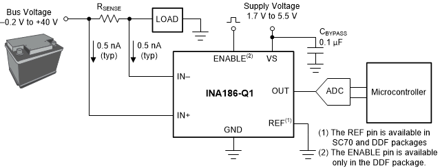
Figure 8-1 shows the basic connections of the INA186-Q1. Place the device as close as possible to the current sense resistor and connect the input pins (IN+ and IN–) to the current sense resistor through kelvin connections.
GUID-20210408-CA0I-DGHN-LQLM-3DHJZHJT26BT-low.gif
To help eliminate ground offset errors between the device and the analog-to-digital converter (ADC), connect the REF pin to the ADC reference input. When driving SAR ADCs, filter or buffer the output of the INA186-Q1 before connecting directly to the ADC.
Figure 8-1 Basic Connections