SBOS612A February   2014  – March 2014 INA225

PRODUCTION DATA.  

  1. Features
  2. Applications
  3. Description
  4. Revision History
  5. Terminal Configuration and Functions
  6. Specifications
    1. 6.1 Absolute Maximum Ratings
    2. 6.2 Handling Ratings
    3. 6.3 Recommended Operating Conditions
    4. 6.4 Thermal Information
    5. 6.5 Electrical Characteristics
    6. 6.6 Typical Characteristics
  7. Detailed Description
    1. 7.1 Overview
    2. 7.2 Functional Block Diagram
    3. 7.3 Feature Description
      1. 7.3.1 Selecting A Shunt Resistor
        1. 7.3.1.1 Selecting A Current-Sense Resistor Example
        2. 7.3.1.2 Optimizing Power Dissipation versus Measurement Accuracy
      2. 7.3.2 Programmable Gain Select
    4. 7.4 Device Functional Modes
      1. 7.4.1 Input Filtering
      2. 7.4.2 Shutting Down the Device
      3. 7.4.3 Using the Device with Common-Mode Transients Above 36 V
  8. Applications and Implementation
    1. 8.1 Application Information
    2. 8.2 Typical Applications
      1. 8.2.1 Microcontroller-Configured Gain Selection
        1. 8.2.1.1 Design Requirements
        2. 8.2.1.2 Detailed Design Procedure
        3. 8.2.1.3 Application Curve
      2. 8.2.2 Unidirectional Operation
        1. 8.2.2.1 Design Requirements
        2. 8.2.2.2 Detailed Design Procedure
        3. 8.2.2.3 Application Curve
      3. 8.2.3 Bidirectional Operation
        1. 8.2.3.1 Design Requirements
        2. 8.2.3.2 Detailed Design Procedure
        3. 8.2.3.3 Application Curve
  9. Power Supply Recommendations
  10. 10Layout
    1. 10.1 Layout Guidelines
    2. 10.2 Layout Example
  11. 11Device and Documentation Support
    1. 11.1 Related Documentation
    2. 11.2 Trademarks
    3. 11.3 Electrostatic Discharge Caution
    4. 11.4 Glossary
  12. 12Mechanical, Packaging, and Orderable Information

パッケージ・オプション

メカニカル・データ(パッケージ|ピン)
サーマルパッド・メカニカル・データ
発注情報

10 Layout

10.1 Layout Guidelines

  • Connect the input terminals to the sensing resistor using a Kelvin or 4-wire connection. This connection technique ensures that only the current-sensing resistor impedance is detected between the input terminals. Poor routing of the current-sensing resistor commonly results in additional resistance present between the input terminals. Given the very low ohmic value of the current resistor, any additional high-current carrying impedance can cause significant measurement errors.
  • The power-supply bypass capacitor should be placed as closely as possible to the supply and ground terminals. The recommended value of this bypass capacitor is 0.1 μF. Additional decoupling capacitance can be added to compensate for noisy or high-impedance power supplies.

10.2 Layout Example

ai_recommended-layout_bos612.gif
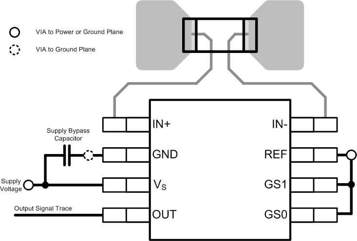
Figure 45. Recommended Layout

The layout shown has REF connected to ground for unidirectional operation. Gain-select terminals (GS0 and GS1) are also connected to ground, indicating a 25-V/V gain setting.