JAJSFI8A July   2018  – December 2018 INA253

PRODUCTION DATA.  

  1. 特長
  2. アプリケーション
  3. 概要
    1.     代表的なアプリケーション
  4. 改訂履歴
  5. Device Comparison Table
  6. Pin Configuration and Functions
    1.     Pin Functions
  7. Specifications
    1. 7.1 Absolute Maximum Ratings
    2. 7.2 ESD Ratings
    3. 7.3 Recommended Operating Conditions
    4. 7.4 Thermal Information
    5. 7.5 Electrical Characteristics
    6. 7.6 Typical Characteristics
  8. Detailed Description
    1. 8.1 Overview
    2. 8.2 Functional Block Diagram
    3. 8.3 Feature Description
      1. 8.3.1 Integrated Shunt Resistor
      2. 8.3.2 Short-Circuit Duration
      3. 8.3.3 Temperature Stability
      4. 8.3.4 Enhanced PWM Rejection Operation
      5. 8.3.5 Input Signal Bandwidth
    4. 8.4 Device Functional Modes
      1. 8.4.1 Adjusting the Output Midpoint With the Reference Pins
      2. 8.4.2 Reference Pin Connections for Unidirectional Current Measurements
      3. 8.4.3 Ground Referenced Output
      4. 8.4.4 Reference Pin Connections for Bidirectional Current Measurements
        1. 8.4.4.1 Output Set to External Reference Voltage
      5. 8.4.5 Output Set to Mid-Supply Voltage
      6. 8.4.6 Output Set to Mid-External Reference
      7. 8.4.7 Output Set Using Resistor Divide
  9. Application and Implementation
    1. 9.1 Application Information
      1. 9.1.1 Input Filtering
    2. 9.2 Typical Applications
      1. 9.2.1 High-Side, High-Drive, Solenoid Current-Sense Application
        1. 9.2.1.1 Design Requirements
        2. 9.2.1.2 Detailed Design Procedure
        3. 9.2.1.3 Application Curve
      2. 9.2.2 Speaker Enhancements and Diagnostics Using Current Sense Amplifier
        1. 9.2.2.1 Design Requirements
        2. 9.2.2.2 Detailed Design Procedure
        3. 9.2.2.3 Application Curve
      3. 9.2.3 Current Sensing for Remote I/Os in PLC
        1. 9.2.3.1 Design Requirements
        2. 9.2.3.2 Application Curve
  10. 10Power Supply Recommendations
  11. 11Layout
    1. 11.1 Layout Guidelines
    2. 11.2 Layout Example
  12. 12デバイスおよびドキュメントのサポート
    1. 12.1 デバイス・サポート
      1. 12.1.1 開発サポート
    2. 12.2 関連資料
    3. 12.3 ドキュメントの更新通知を受け取る方法
    4. 12.4 コミュニティ・リソース
    5. 12.5 商標
    6. 12.6 静電気放電に関する注意事項
    7. 12.7 Glossary
  13. 13メカニカル、パッケージ、および注文情報

パッケージ・オプション

メカニカル・データ(パッケージ|ピン)
サーマルパッド・メカニカル・データ
発注情報

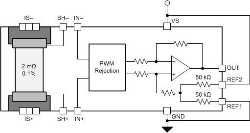
Output Set to Mid-Supply Voltage

Figure 36 shows that by connecting one reference pin to VS and the other to the GND pin, the output is set at half of the supply when there is no differential input. This method creates a ratiometric offset to the supply voltage, where the output voltage remains at VS / 2 when 0 V is applied between the IN+ and IN– inputs.
INA253 ina253-mid-supply-voltage-output.gifFigure 36. Mid-Supply Voltage Output