JAJSM04A june 2021 – march 2023 INA254
PRODUCTION DATA
- 1 特長
- 2 アプリケーション
- 3 概要
- 4 Revision History
- 5 Device Comparison
- 6 Pin Configuration and Functions
- 7 仕様
-
8 Detailed Description
- 8.1 Overview
- 8.2 Functional Block Diagram
- 8.3 Feature Description
- 8.4
Device Functional Modes
- 8.4.1 Adjusting the Output Midpoint With the Reference Pins
- 8.4.2 Reference Pin Connections for Unidirectional Current Measurements
- 8.4.3 Ground Referenced Output
- 8.4.4 Reference Pin Connections for Bidirectional Current Measurements
- 8.4.5 Output Set to Mid-Supply Voltage
- 8.4.6 Output Set to Mid-External Reference
- 8.4.7 Output Set Using Resistor Divider
- 9 Application and Implementation
- 10Device and Documentation Support
- 11Mechanical, Packaging, and Orderable Information
9.1.1 Input Filtering
Input filters are not required for accurate measurements using the INA254. For most accurate results, do not use filters at the IN+ and IN– inputs. However, If filter components are used on the input of the amplifier, follow the guidelines in this section to minimize effects on performance.
Based strictly on user design requirements, external filtering of the current signal may be desired. The initial location that can be considered for the filter is at the output of the current amplifier. Although placing the filter at the output satisfies the filtering requirements, this location changes the low output impedance measured by any circuitry connected to the output voltage pin. The other location for filter placement is at the current amplifier input pins. This location also satisfies the filtering requirement, but carefully select the components to minimize the impact on device performance. Figure 9-1 shows a filter placed at the inputs pins.
 Figure 9-1 Filter at
Input Pins
Figure 9-1 Filter at
Input PinsExternal series resistance provides a source of additional measurement error. Therefore, keep the value of these series resistors to 10 Ω or less to reduce loss of accuracy. The internal bias network shown in Figure 9-1 creates a mismatch in input bias currents when a differential voltage is applied between the input pins (see Figure 9-2). If additional external series filter resistors are added to the circuit, a mismatch is created in the voltage drop across the filter resistors. This voltage is a differential error voltage in the shunt resistor voltage. In addition to the absolute resistor value, mismatch resulting from resistor tolerance can significantly impact the error because this value is calculated based on the actual measured resistance.
 Figure 9-2 Input Bias Current vs
Differential Input Voltage
Figure 9-2 Input Bias Current vs
Differential Input VoltageUse Equation 1 to calculate the measurement error expected from the additional external filter resistors.

where
- Equation 2 determines the Gain Error Factor
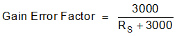
Where:
- RS is the external filter resistance value
Use Equation 2 to calculate the gain error factor and determine the gain error introduced by the additional external series resistance. Use Equation 1 to calculate the deviation of the shunt voltage resulting from the attenuation and imbalance created by the added external filter resistance. Table 9-1 provides the gain error factor and gain error for several resistor values.
| EXTERNAL RESISTANCE (Ω) | GAIN ERROR FACTOR | GAIN ERROR (%) |
|---|---|---|
| 5 | 0.998 | 0.17 |
| 10 | 0.997 | 0.33 |
| 100 | 0.968 | 3.23 |