JAJSCW1C July 2016 – December 2016 INA260
PRODUCTION DATA.
- 1 特長
- 2 アプリケーション
- 3 概要
- 4 改訂履歴
- 5 Related Products
- 6 Pin Configuration and Functions
- 7 Specifications
-
8 Detailed Description
- 8.1 Overview
- 8.2 Functional Block Diagram
- 8.3 Feature Description
- 8.4 Device Functional Modes
- 8.5 Programming
- 8.6
Register Maps
- 8.6.1 Configuration Register (00h) (Read/Write)
- 8.6.2 Current Register (01h) (Read-Only)
- 8.6.3 Bus Voltage Register (02h) (Read-Only)
- 8.6.4 Power Register (03h) (Read-Only)
- 8.6.5 Mask/Enable Register (06h) (Read/Write)
- 8.6.6 Alert Limit Register (07h) (Read/Write)
- 8.6.7 Manufacturer ID Register (FEh) (Read-Only)
- 8.6.8 Die ID Register (FFh) (Read-Only)
- 9 Application and Implementation
- 10Power Supply Recommendations
- 11Layout
- 12デバイスおよびドキュメントのサポート
- 13メカニカル、パッケージ、および注文情報
7 Specifications
7.1 Absolute Maximum Ratings
over operating free-air temperature range (unless otherwise noted)(1)| MIN | MAX | UNIT | ||
|---|---|---|---|---|
| Analog input current | Continuous Conduction | ±15 | A | |
| Analog inputs: IN+, IN– | Common-mode (VIN+ + VIN–) / 2 | –0.3 | 40 | V |
| Voltage | Supply, VS | 6 | V | |
| VBUS pin | –0.3 | 40 | ||
| SDA, SCL, ALERT | –0.3 | 6 | ||
| Address Pins, A0, A1 | –0.3 | VS + 0.3 | ||
| Open-drain digital output current, IOUT | 10 | mA | ||
| Temperature | Junction, TJ | 150 | °C | |
| Storage, Tstg | –65 | 150 | ||
(1) Stresses beyond those listed under Absolute Maximum Ratings may cause permanent damage to the device. These are stress ratings only, which do not imply functional operation of the device at these or any other conditions beyond those indicated under Recommended Operating Conditions. Exposure to absolute-maximum-rated conditions for extended periods may affect device reliability.
7.2 ESD Ratings
| VALUE | UNIT | |||
|---|---|---|---|---|
| V(ESD) | Electrostatic discharge | Human body model (HBM), per ANSI/ESDA/JEDEC JS-001(1) | ±2000 | V |
| Charged device model (CDM), per JEDEC specification JESD22-C101(2) | ±1000 | |||
(1) JEDEC document JEP155 states that 500-V HBM allows safe manufacturing with a standard ESD control process.
(2) JEDEC document JEP157 states that 250-V CDM allows safe manufacturing with a standard ESD control process.
7.3 Recommended Operating Conditions
over operating free-air temperature range (unless otherwise noted)| MIN | NOM | MAX | UNIT | ||
|---|---|---|---|---|---|
| VCM | Common-mode input voltage | 0 | 36 | V | |
| VS | Operating supply voltage | 2.7 | 5.5 | V | |
| TA | Operating free-air temperature | –40 | 125 | °C | |
7.4 Thermal Information
| THERMAL METRIC(1) | INA260 | UNIT | |
|---|---|---|---|
| PW (TSSOP) | |||
| 16 PINS | |||
| RθJA | Junction-to-ambient thermal resistance | 115.6 | °C/W |
| RθJC(top) | Junction-to-case (top) thermal resistance | 50.1 | °C/W |
| RθJB | Junction-to-board thermal resistance | 46.8 | °C/W |
| ψJT | Junction-to-top characterization parameter | 3.3 | °C/W |
| ψJB | Junction-to-board characterization parameter | 46.5 | °C/W |
| RθJC(bot) | Junction-to-case (bottom) thermal resistance | N/A | °C/W |
(1) For more information about traditional and new thermal metrics, see the Semiconductor and IC Package Thermal Metrics application report, SPRA953.
7.5 Electrical Characteristics
at TA = 25°C, VS = 3.3 V, VIN+ = 12 V, VSENSE = (VIN+ – VIN–) = 0 mV and VVBUS = 12 V (unless otherwise noted)| PARAMETER | TEST CONDITIONS | MIN | TYP | MAX | UNIT | ||
|---|---|---|---|---|---|---|---|
| INPUT | |||||||
| VCM | Common-mode input range | 0 | 36 | V | |||
| Bus voltage input range(1) | 0 | 36 | V | ||||
| CMRR | Common-mode rejection | 0 V ≤ VIN+ ≤ 36 V | 0 | 150 | µA/V | ||
| IOS | Current sense offset, RTI(2) | ±1.25 | ±5 | mA | |||
| Current sense offset drift, RTI(2) | –40°C ≤ TA ≤ 125°C | 1 | 50 | µA/°C | |||
| PSRR | Current sense offset voltage, RTI(2) vs power supply | 2.7 V ≤ VS ≤ 5.5 V | 1.6 | 3 | mA/V | ||
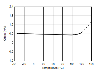
| VOS | Bus offset voltage, RTI(2) | ±1.25 | ±7.5 | mV | |||
| Bus offset voltage, RTI(2) vs temperature | –40°C ≤ TA ≤ 125°C | 0.6 | 40 | µV/°C | |||
| PSRR | Bus offset voltage, RTI(2) vs power supply | 1.5 | mV/V | ||||
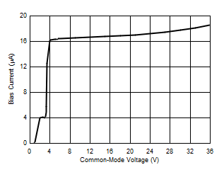
| IB | Input bias current (IIN+, IIN– pins) | (IN+ pin) + (IN– pin), ISENSE = 0A | 17 | µA | |||
| VBUS input impedance | 830 | kΩ | |||||
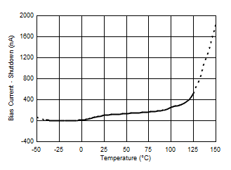
| Input leakage(3) | (IN+ pin) + (IN– pin), power-down mode |
0.1 | 0.5 | µA | |||
| DC ACCURACY | |||||||
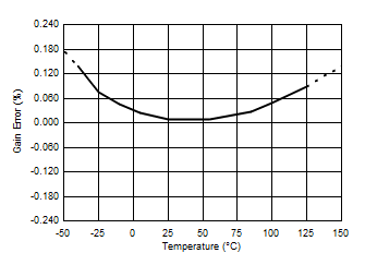
| System current sense gain error | ISENSE = –15 A to 15 A, TA = 25°C | 0.02% | 0.15% | ||||
| ISENSE = –10 A to 10 A, –40°C ≤ TA ≤ 125°C |
0.2% | 0.5% | |||||
| –40°C ≤ TA ≤ 125°C | 10 | 35 | ppm/°C | ||||
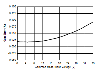
| Bus voltage gain error | VBUS = 0 V to 36 V, TA = 25°C | 0.02% | 0.1% | ||||
| VBUS = 0 V to 36 V, –40°C ≤ TA ≤ 125°C |
0.1% | 0.4% | |||||
| –40°C ≤ TA ≤ 125°C | 15 | 40 | ppm/°C | ||||
| INTEGRATED ADC | |||||||
| ADC native resolution | 16 | Bits | |||||
| 1-LSB step size | Current | 1.25 | mA | ||||
| Bus voltage | 1.25 | mV | |||||
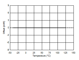
| Power | 10 | mW | |||||
| tCT | ADC conversion time | CT bit = 000 | 140 | 154 | µs | ||
| CT bit = 001 | 204 | 224 | |||||
| CT bit = 010 | 332 | 365 | |||||
| CT bit = 011 | 588 | 646 | |||||
| CT bit = 100 | 1.1 | 1.21 | ms | ||||
| CT bit = 101 | 2.116 | 2.328 | |||||
| CT bit = 110 | 4.156 | 4.572 | |||||
| CT bit = 111 | 8.244 | 9.068 | |||||
| Differential nonlinearity | ±0.1 | LSB | |||||
| INTEGRATED SHUNT | |||||||
| Package resistance | IN+ to IN– | 4.5 | mΩ | ||||
| Maximum continuous current | –40°C ≤ TA ≤ 85°C | ±15 | A | ||||
| Short time overload change | ISENSE = 30 A for 5 seconds | ±0.05% | |||||
| Change due to thermal shock | –65°C ≤ TA ≤ 150°C, 500 cycles | ±0.1% | |||||
| Resistance change to solder heat | 260°C solder, 10 s | ±0.1% | |||||
| High temperature exposure change | 1000 hours, TA = 150°C | ±0.15% | |||||
| Cold temperature storage change | 24 hours, TA = –65°C | ±0.025% | |||||
| SMBus | |||||||
| SMBus timeout(4) | 28 | 35 | ms | ||||
| DIGITAL INPUT/OUTPUT | |||||||
| Input capacitance | 3 | pF | |||||
| Leakage input current | 0 V ≤ VSCL ≤ VS, 0 V ≤ VSDA ≤ VS, 0 V ≤ VALERT ≤ VS, 0 V ≤ VA0 ≤ VS, 0 V ≤ VA1 ≤ VS |
0.1 | 1 | µA | |||
| VIH | High-level input voltage | 0.7 × VS | 6 | V | |||
| VIL | Low-level input voltage | 0 | 0.3 × VS | V | |||
| VOL | Low-level output voltage, SDA, ALERT | IOL = 3 mA | 0 | 0.4 | V | ||
| SDA, SCL Hysteresis | 500 | mV | |||||
| POWER SUPPLY | |||||||
| Operating supply range | 2.7 | 5.5 | V | ||||
| IQ | Quiescent current | 310 | 420 | µA | |||
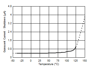
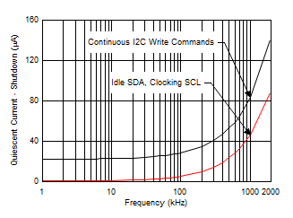
| Quiescent current, power-down (shutdown) mode | 0.5 | 2 | µA | ||||
| VPOR | Power-on reset threshold | 2 | V | ||||
(1) Although the input range is 36 V, the full-scale range of the ADC scaling is 40.96 V; see the Basic ADC Functions section. Do not apply more than 36 V.
(2) RTI = Referred-to-input.
(3) Input leakage is positive (current flowing into the pin) for the conditions shown at the top of this table. Negative leakage currents can occur under different input conditions.
(4) SMBus timeout in the INA260 resets the interface any time SCL is low for more than 28 ms.
7.6 Typical Characteristics
At TA = 25°C, VS = 3.3 V, VIN+ = 12 V, VSENSE = (VIN+ – VIN–) = 0 mV and VVBUS = 12 V, unless otherwise noted.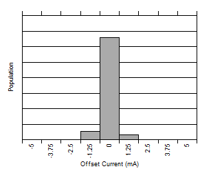
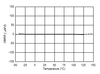
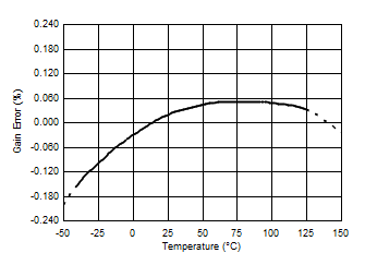
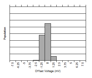
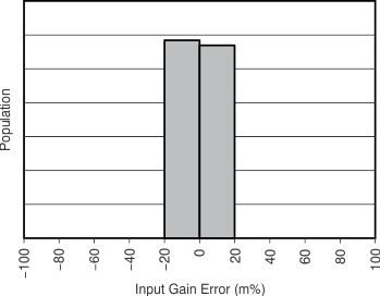
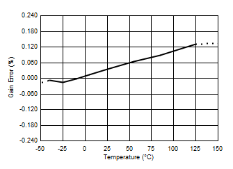
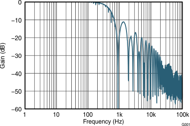
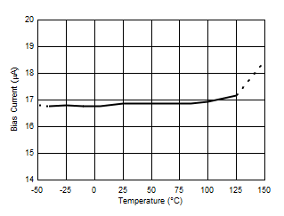
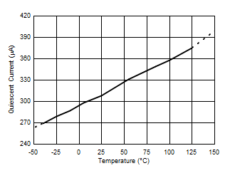
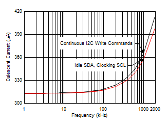
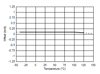
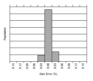 Figure 4. Current Sense Gain Error Production Distribution
