JAJSI20B september   2019  – june 2023 INA333-Q1

PRODUCTION DATA  

  1.   1
  2. 特長
  3. アプリケーション
  4. 概要
  5. Revision History
  6. Pin Configuration and Functions
  7. Specifications
    1. 6.1 Absolute Maximum Ratings
    2. 6.2 ESD Ratings
    3. 6.3 Recommended Operating Conditions
    4. 6.4 Thermal Information
    5. 6.5 Electrical Characteristics
    6. 6.6 Typical Characteristics
  8. Detailed Description
    1. 7.1 Overview
    2. 7.2 Functional Block Diagram
    3. 7.3 Feature Description
      1. 7.3.1 Internal Offset Correction
      2. 7.3.2 Input Protection
    4. 7.4 Device Functional Modes
  9. Application and Implementation
    1. 8.1 Application Information
      1. 8.1.1 Input Common-Mode Range
    2. 8.2 Typical Application
      1. 8.2.1 Design Requirements
      2. 8.2.2 Detailed Design Procedure
        1. 8.2.2.1 Setting the Gain
        2. 8.2.2.2 Offset Trimming
        3. 8.2.2.3 Noise Performance
        4. 8.2.2.4 Input Bias Current Return Path
        5. 8.2.2.5 Low Voltage Operation
        6. 8.2.2.6 Single-Supply Operation
      3. 8.2.3 Application Curves
    3. 8.3 Power Supply Recommendations
    4. 8.4 Layout
      1. 8.4.1 Layout Guidelines
      2. 8.4.2 Layout Example
  10. Device and Documentation Support
    1. 9.1 Device Support
      1. 9.1.1 Development Support
        1. 9.1.1.1 TINA-TI Simulation Software (Free Download)
    2. 9.2 Documentation Support
      1. 9.2.1 Related Documentation
    3. 9.3 ドキュメントの更新通知を受け取る方法
    4. 9.4 サポート・リソース
    5. 9.5 Trademarks
    6. 9.6 静電気放電に関する注意事項
    7. 9.7 用語集
  11. 10Mechanical, Packaging, and Orderable Information

パッケージ・オプション

メカニカル・データ(パッケージ|ピン)
サーマルパッド・メカニカル・データ
発注情報

Offset Trimming

Most applications require no external offset adjustment. However, if necessary, adjustments can be made by applying a voltage to the REF pin. Figure 8-2 shows an optional circuit for trimming the output offset voltage. The voltage applied to REF pin is summed at the output. The operational amplifier buffer provides low impedance at the REF pin to preserve good common-mode rejection.
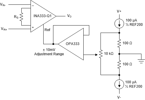
GUID-A56E92EC-FEDC-4C72-B722-467F25A43F94-low.gifFigure 8-2 Optional Trimming of Output Offset Voltage