JAJSPA2C december 2022 – may 2023 INA351
PRODUCTION DATA
- 1
- 1 特長
- 2 アプリケーション
- 3 概要
- 4 Revision History
- 5 Device Comparison Table
- 6 Pin Configuration and Functions
- 7 Specifications
- 8 Detailed Description
- 9 Application and Implementation
- 10Device and Documentation Support
- 11Mechanical, Packaging, and Orderable Information
パッケージ・オプション
メカニカル・データ(パッケージ|ピン)
サーマルパッド・メカニカル・データ
- DSG|8
発注情報
8.3.2 Input Common-Mode Voltage Range
INA351 has two gain stages, the first stage has a common-mode gain of 1 and a differential gain set by the GS pin. The second stage is configured in a difference-amplifier configuration with differential gain of 1 and ideally rejects all of the input common mode completely. The second stage also provides a gain of 1 from REF pin to set the output common-mode voltage.
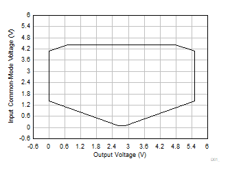
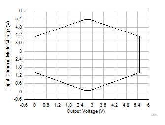
The linear input voltage range of the INA351, even for a rail-to-rail first stage, is dictated by both the signal swing at output of the first stage as well as the input common-mode voltage range output swing of the second stage. In order to maximize performance, it is critical to keep the INA351 within its linear range for a given combination of gain, reference, and input common-mode voltage for a particular input differential. Input common-mode voltage (VCM) vs output voltage graphs (VOUT) in this section show a particular reference voltage and gain configuration to outline the linear performance region of INA351. A good common-mode rejection can be expected when operating with in the limits of the VCM vs VOUT graph. Note that the INA351 linear input voltage cannot be close to or extend beyond the supply rails, as the output of the first stage will be driven into saturation.
The common-mode range for the most common operating conditions is outlined as follows. Figure 8-66 shows the region of operation where a minimum of 86 dB can be achieved. Figure 8-67 has much wider region of operation with a lower minimum CMRR of 62 dB, because the input signal crosses over the transition region of the input pairs to achieve rail-to-rail operation. The common-mode range for other operating conditions is best calculated with the INA VCM vs VOUT tool located under the Amplifiers and Comparators section of the Analog Engineer's Calculator on ti.com. INA351-HCM model can be specifically used for applications requiring high CMRR and corresponds to performance shown in Figure 8-66. INA351xxS model can be used for applications where the input common mode can be expected to vary rail-to-rail and the model corresponds to performance shown in Figure 8-67 where CMRR drops to 62-dB minimum.

| VS = 5.5 V | G = 10, 20, 30, 50 | VREF = VS / 2 |

| VS = 5.5 V | G = 10, 20, 30, 50 | VREF = VS / 2 |