JAJSEX6B December 2017 – October 2019 INA381
PRODUCTION DATA.
- 1 特長
- 2 アプリケーション
- 3 概要
- 4 改訂履歴
- 5 概要(続き)
- 6 Pin Configuration and Functions
- 7 Specifications
- 8 Detailed Description
- 9 Applications and Implementation
- 10Power Supply Recommendations
- 11Layout
- 12デバイスおよびドキュメントのサポート
- 13メカニカル、パッケージ、および注文情報
パッケージ・オプション
デバイスごとのパッケージ図は、PDF版データシートをご参照ください。
メカニカル・データ(パッケージ|ピン)
- DGS|10
- DSG|8
サーマルパッド・メカニカル・データ
- DSG|8
発注情報
9.1.3 Operation With Common-Mode Transients Greater Than 26 V
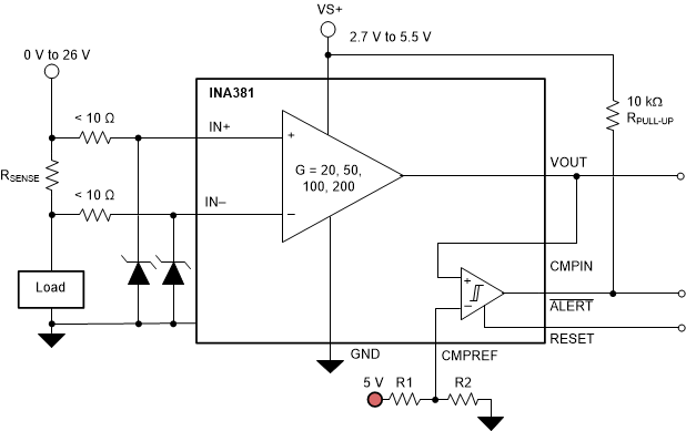
With a small amount of additional circuitry, the INA381 can be used in circuits subject to transients greater than 26 V. Use only Zener diodes or Zener-type transient absorbers (sometimes referred to as transorbs)—any other type of transient absorber has an unacceptable time delay. Start by adding a pair of resistors as shown in Figure 47 as a working impedance for the Zener diode. Keep these resistors as small as possible; most often approximately 10 Ω. Larger values can be used with an effect on gain that is discussed in the Input Filteringsection. This circuit limits only short-term transients and, therefore, many applications are satisfied with a 10-Ω resistor along with conventional Zener diodes of the lowest acceptable power rating. This combination uses the least amount of board space. These diodes can be found in packages as small as SOT-523 or SOD-523.
 Figure 47. Transient Protection
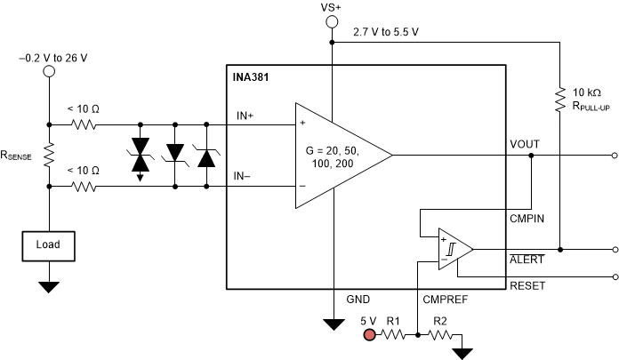
 In the event that low-power Zener diodes do not have sufficient transient absorption capability, use a higher-power transorb. Figure 47 shows that the most package-efficient solution involves using a single transorb and back-to-back diodes between the device inputs. The most space-efficient solutions are dual, series-connected diodes in a single SOT-523 or SOD-523 package. In either of the examples provided in Figure 47 and Figure 48, the total board area required by the INA381 with all protective components is less than that of an SOIC-8 package, and only slightly greater than that of a VSSOP-8 package.
 Figure 48. Transient Protection Using a Single Transorb and Input Clamps