SBOS631B June 2012 – November 2017 INA827
PRODUCTION DATA.
- 1 Features
- 2 Applications
- 3 Description
- 4 Revision History
- 5 Pin Configuration and Functions
- 6 Specifications
- 7 Typical Characteristics
- 8 Detailed Description
- 9 Application and Implementation
- 10Power Supply Recommendations
- 11Layout
- 12Device and Documentation Support
- 13Mechanical, Packaging, and Orderable Information
11 Layout
11.1 Layout Guidelines
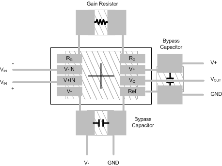
Attention to good layout practices is always recommended. Keep traces short and, when possible, use a printed circuit board (PCB) ground plane with surface-mount components placed as close to the device pins as possible. Place 0.1-μF bypass capacitors close to the supply pins. Apply these guidelines throughout the analog circuit to improve performance and provide benefits such as reducing the electromagnetic-interference (EMI) susceptibility.
11.1.1 CMRR vs Frequency
The INA827 pinout is optimized for achieving maximum CMRR performance over a wide range of frequencies. However, care must be taken to ensure that both input paths are well-matched for source impedance and capacitance to avoid converting common-mode signals into differential signals. In addition, parasitic capacitance at the gain-setting pins can also affect CMRR over frequency. For example, in applications that implement gain switching using switches or PhotoMOS® relays to change the value of RG, choose the component so that the switch capacitance is as small as possible.
11.2 Layout Example
 Figure 65. INA827 Example Layout