JAJSIR4A March 2020 – July 2020 ISO1044
PRODUCTION DATA
- 1 特長
- 2 アプリケーション
- 3 概要
- 4 Revision History
- 5 Pin Configuration and Functions
-
6 Specifications
- 6.1 Absolute Maximum Ratings
- 6.2 ESD Ratings
- 6.3 Recommended Operating Conditions
- 6.4 Thermal Information
- 6.5 Power Ratings
- 6.6 Insulation Specifications
- 6.7 Safety-Related Certifications
- 6.8 Safety Limiting Values
- 6.9 Electrical Characteristics - DC Specification
- 6.10 Switching Characteristics
- 6.11 Insulation Characteristics Curves
- 6.12 Typical Characteristics
- 7 Parametric Measurement Information
- 8 Detailed Description
- 9 Application and Implementation
- 10Power Supply Recommendations
- 11Layout
- 12Device and Documentation Support
- 13Mechanical, Packaging, and Orderable Information
パッケージ・オプション
デバイスごとのパッケージ図は、PDF版データシートをご参照ください。
メカニカル・データ(パッケージ|ピン)
- D|8
サーマルパッド・メカニカル・データ
発注情報
7 Parametric Measurement Information
 Figure 7-1 Driver Voltage, Current and Test Definitions
 Figure 7-2 Bus Logic State Voltage Definitions
Figure 7-3 Driver Test Circuit and Voltage Waveforms. 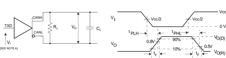
The input pulse is supplied by a generator having the following characteristics: PRR ≤ 125 kHz, 50% duty cycle, tr ≤ 6 ns, tf ≤ 6 ns, ZO = 50 Ω.
 Figure 7-4 Receiver Voltage and Current Definitions
The input pulse is supplied by a generator having the following characteristics: PRR ≤ 125 kHz, 50% duty cycle,
tr ≤ 6 ns, tf ≤ 6 ns, ZO = 50 Ω.
Figure 7-5 Receiver Test Circuit and Voltage Waveformstr ≤ 6 ns, tf ≤ 6 ns, ZO = 50 Ω.
Table 7-1 Receiver Differential Input Voltage Threshold Test
| INPUT | OUTPUT | |||
|---|---|---|---|---|
| VCANH | VCANL | |VID| | RXD | |
| -11.5 V | -12.5 V | 1000 mV | L | VOL |
| 12.5 V | 11.5 V | 1000 mV | L | |
| -8.55 V | -9.45 V | 900 mV | L | |
| 9.45 V | 8.55 V | 900 mV | L | |
| -8.75 V | -9.25 V | 500 mV | H | VOH |
| 9.25 V | 8.75 V | 500 mV | H | |
| -11.8 V | -12.2 V | 400 mV | H | |
| 12.2 V | 11.8 V | 400 mV | H | |
| Open | Open | X | H | |
 Figure 7-6 tLOOP and CAN
FD Timing Parameter Measurement
Figure 7-6 tLOOP and CAN
FD Timing Parameter Measurement
The input pulse is supplied by a
generator having the following characteristics: tr ≤ 6 ns,
tf ≤ 6 ns, ZO = 50 Ω.
Figure 7-7 Dominant
Time-out Test Circuit and Voltage Waveforms Figure 7-8 Driver Short-Circuit Current Test Circuit and Waveforms
 Figure 7-9 Common-Mode Transient Immunity Test Circuit