SLLSER7 November 2015 ISO7330-Q1 , ISO7331-Q1
PRODUCTION DATA.
- 1 Features
- 2 Applications
- 3 Description
- 4 Revision History
- 5 Pin Configuration and Functions
-
6 Specifications
- 6.1 Absolute Maximum Ratings
- 6.2 ESD Ratings
- 6.3 Recommended Operating Conditions
- 6.4 Thermal Information
- 6.5 Electrical Characteristics—5-V Supply
- 6.6 Supply Current Characteristics—5-V Supply
- 6.7 Electrical Characteristics—3.3-V Supply
- 6.8 Supply Current Characteristics—3.3-V Supply
- 6.9 Power Dissipation Characteristics
- 6.10 Switching Characteristics—5-V Supply
- 6.11 Switching Characteristics—3.3-V Supply
- 6.12 Typical Characteristics
- 7 Parameter Measurement Information
- 8 Detailed Description
- 9 Application and Implementation
- 10Power Supply Recommendations
- 11Layout
- 12Device and Documentation Support
- 13Mechanical, Packaging, and Orderable Information
パッケージ・オプション
デバイスごとのパッケージ図は、PDF版データシートをご参照ください。
メカニカル・データ(パッケージ|ピン)
- DW|16
サーマルパッド・メカニカル・データ
発注情報
9 Application and Implementation
NOTE
Information in the following applications sections is not part of the TI component specification, and TI does not warrant its accuracy or completeness. TI’s customers are responsible for determining suitability of components for their purposes. Customers should validate and test their design implementation to confirm system functionality.
9.1 Application Information
The ISO733x-Q1 family of devices uses single-ended TTL-logic switching technology. Its supply voltage range is from 3 V to 5.5 V for both supplies, VCC1 and VCC2. When designing with digital isolators, keep in mind that because of the single-ended design structure, digital isolators do not conform to any specific interface standard and are only intended for isolating single-ended CMOS or TTL digital signal lines. The isolator is typically placed between the data controller (that is, μC or UART), and a data converter or a line transceiver, regardless of the interface type or standard.
9.2 Typical Application
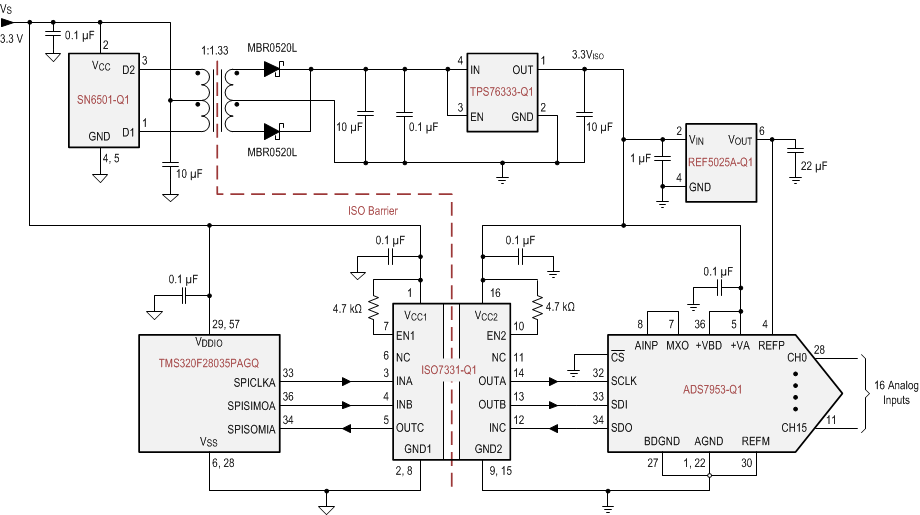
The ISO7331-Q1 device combined with Texas Instruments' Piccolo™ microcontroller, analog-to-digital receiver, transformer driver, and voltage regulator can create an isolated serial peripheral interface (SPI) as shown in Figure 18.
9.2.1 Design Requirements
9.2.1.1 Typical Supply Current Equations
For the equations in this section, the following is true:
- ICC1 and ICC2 are typical supply currents measured in mA
- f is the data rate measured in Mbps
- CL is the capacitive load measured in pF
9.2.1.1.1 ISO7330-Q1
At VCC1 = VCC2 = 5 V
At VCC1 = VCC2 = 3.3 V
9.2.1.1.2 ISO7321-Q1
At VCC1 = VCC2 = 5 V
At VCC1 = VCC2 = 3.3 V
9.2.2 Detailed Design Procedure
9.2.2.1 Electromagnetic Compatibility (EMC) Considerations
Many applications in harsh industrial environment are sensitive to disturbances such as electrostatic discharge (ESD), electrical fast transient (EFT), surge and electromagnetic emissions. These electromagnetic disturbances are regulated by international standards such as IEC 61000-4-x and CISPR 22. Although system-level performance and reliability depends, to a large extent, on the application board design and layout, the ISO733x-Q1 family of devices incorporates many chip-level design improvements for overall system robustness. Some of these improvements include:
- Robust ESD protection cells for input and output signal pins and inter-chip bond pads.
- Low-resistance connectivity of ESD cells to supply and ground pins.
- Enhanced performance of high voltage isolation capacitor for better tolerance of ESD, EFT and surge events.
- Bigger on-chip decoupling capacitors to bypass undesirable high energy signals through a low impedance path.
- PMOS and NMOS devices isolated from each other by using guard rings to avoid triggering of parasitic SCRs.
- Reduced common mode currents across the isolation barrier by ensuring purely differential internal operation.
9.2.3 Application Curves
The following typical eye diagrams of the ISO733x-Q1 family of devices indicate low jitter and wide open eye at the maximum data rate of 25 Mbps.
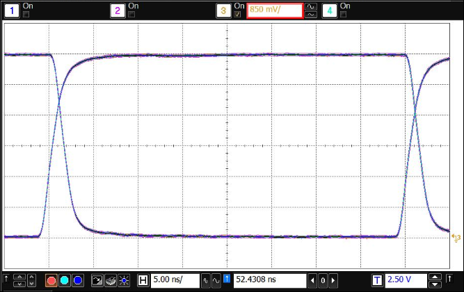 Figure 19. Eye Diagram at 25 Mbps, 5 V and 25°C
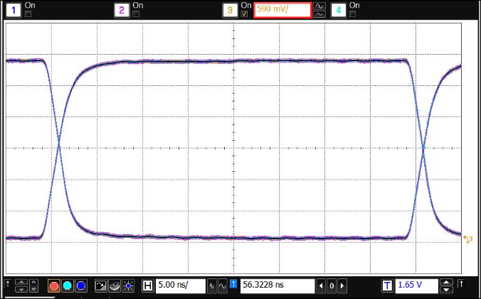 Figure 20. Eye Diagram at 25 Mbps, 3.3 V and 25°C
9.2.4 Systems Examples
Unlike optocouplers, which require external components to improve performance, provide bias, or limit current, the ISO733x-Q1 family of devices only requires two external bypass capacitors to operate.
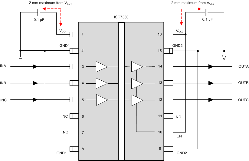 Figure 21. Typical ISO7330-Q1 Circuit Hook-up
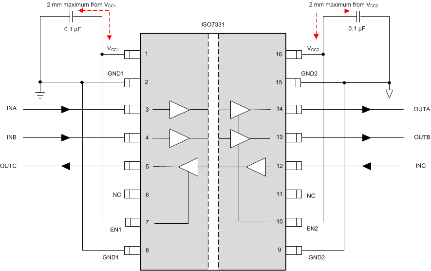 Figure 22. Typical ISO7331-Q1 Circuit Hook-up