SLLS984I June 2009 – July 2015 ISO7420 , ISO7420M , ISO7421
UNLESS OTHERWISE NOTED, this document contains PRODUCTION DATA.
- 1 Features
- 2 Applications
- 3 Description
- 4 Revision History
- 5 Pin Configuration and Functions
-
6 Specifications
- 6.1 Absolute Maximum Ratings
- 6.2 ESD Ratings
- 6.3 Recommended Operating Conditions
- 6.4 Thermal Information
- 6.5 Electrical Characteristics: VCC1 and VCC2 at 5 V ±5%
- 6.6 Electrical Characteristics: VCC1 at 5 V ±5%, VCC2 at 3.3 V ±5%
- 6.7 Electrical Characteristics: VCC1 at 3.3 V ±5%, VCC2 at 5 V ±5%
- 6.8 Electrical Characteristics: VCC1 and VCC2 at 3.3 V ±5%
- 6.9 Power Dissipation Characteristics
- 6.10 Switching Characteristics: VCC1 and VCC2 at 5 V ±5%
- 6.11 Switching Characteristics: VCC1 at 5 V ±5%, VCC2 at 3.3 V ±5%
- 6.12 Switching Characteristics: VCC1 at 3.3 V ±5%, VCC2 at 5 V ±5%
- 6.13 Switching Characteristics: VCC1 and VCC2 at 3.3 V ±5%
- 6.14 Typical Characteristics
- 7 Parameter Measurement Information
- 8 Detailed Description
- 9 Application and Implementation
- 10Power Supply Recommendations
- 11Layout
- 12Device and Documentation Support
- 13Mechanical, Packaging, and Orderable Information
6 Specifications
6.1 Absolute Maximum Ratings
| See (1) | MIN | MAX | UNIT | ||||
|---|---|---|---|---|---|---|---|
| VCC | Supply voltage(2), VCC1, VCC2 | –0.5 | 6 | V | |||
| VI | Voltage at IN, OUT | –0.5 | VCC + 0.5(3) | V | |||
| IO | Output current | –15 | 15 | mA | |||
| TJ(max) | Maximum junction temperature | 150 | °C | ||||
| Tstg | Storage temperature | –65 | 150 | °C | |||
(1) Stresses beyond those listed under Absolute Maximum Ratings may cause permanent damage to the device. These are stress ratings only and functional operation of the device at these or any other conditions beyond those indicated under Recommended Operating Conditions is not implied. Exposure to absolute-maximum-rated conditions for extended periods may affect device reliability.
(2) All voltage values except differential I/O bus voltages are with respect to network ground terminal and are peak voltage values.
(3) Maximum voltage must not exceed 6 V.
6.2 ESD Ratings
| VALUE | UNIT | |||
|---|---|---|---|---|
| V(ESD) | Electrostatic discharge | Human body model (HBM), per ANSI/ESDA/JEDEC JS-001(1) | ±4000 | V |
| Field-induced charged-device model, JEDEC Standard 22, Test Method C101 | ±1500 | |||
| Machine model, ANSI/ESDS5.2-1996 | ±200 | |||
(1) JEDEC document JEP155 states that 500-V HBM allows safe manufacturing with a standard ESD control process.
6.3 Recommended Operating Conditions
| MIN | NOM | MAX | UNIT | |||
|---|---|---|---|---|---|---|
| VCC1, VCC2 | Supply voltage - 3.3-V operation | 3.15 | 3.3 | 3.45 | V | |
| Supply voltage - 5-V operation | 4.75 | 5 | 5.25 | |||
| IOH | High-level output current | –4 | mA | |||
| IOL | Low-level output current | 4 | mA | |||
| VIH | High-level input voltage | 2 | 5.25 | V | ||
| VIL | Low-level input voltage | 0 | 0.8 | V | ||
| 1/tui | Signaling rate | 0 | 1 | Mbps | ||
| tui | Input pulse duration | 1 | us | |||
| TJ(1) | Junction temperature | –40 | 136 | °C | ||
| TA | Ambient temperature | ISO7420, ISO7421 | -40 | 25 | 105 | °C |
| ISO7420M | -40 | 25 | 125 | |||
(1) To maintain the recommended operating conditions for TJ, see the Thermal Information.
6.4 Thermal Information
| THERMAL METRIC(1) | ISO742x | UNIT | ||
|---|---|---|---|---|
| D (SOIC) | ||||
| 8 PINS | ||||
| RθJA | Junction-to-ambient thermal resistance | Low-K Board | 212 | °C/W |
| High-K Board | 116.6 | |||
| RθJC(top) | Junction-to-case (top) thermal resistance | 71.6 | °C/W | |
| RθJB | Junction-to-board thermal resistance | 57.3 | °C/W | |
| ψJT | Junction-to-top characterization parameter | 28.3 | °C/W | |
| ψJB | Junction-to-board characterization parameter | 56.8 | °C/W | |
(1) For more information about traditional and new thermal metrics, see the Semiconductor and IC Package Thermal Metrics application report, SPRA953.
6.5 Electrical Characteristics: VCC1 and VCC2 at 5 V ±5%
TA = –40°C to 125°C for ISO7420M, TA = –40°C to 105°C for ISO742x| PARAMETER | TEST CONDITIONS | MIN | TYP | MAX | UNIT | ||
|---|---|---|---|---|---|---|---|
| VOH | High-level output voltage | IOH = –4 mA; see Figure 6. | VCCO(1) – 0.8 | 4.6 | V | ||
| IOH = –20 μA; see Figure 6. | VCCO – 0.1 | 5 | |||||
| VOL | Low-level output voltage | IOL = 4 mA; see Figure 6. | 0.2 | 0.4 | V | ||
| IOL = 20 μA; see Figure 6. | 0 | 0.1 | |||||
| VI(HYS) | Input threshold voltage hysteresis | 400 | mV | ||||
| IIH | High-level input current | INx at 0 V or VCCI(1) | 10 | μA | |||
| IIL | Low-level input current | –10 | μA | ||||
| CMTI | Common-mode transient immunity | VI = VCCI or 0 V; see Figure 8. | 25 | 50 | kV/μs | ||
| SUPPLY CURRENT (ALL INPUTS SWITCHING WITH SQUARE WAVE CLOCK SIGNAL FOR DYNAMIC ICC MEASUREMENT) | |||||||
| ISO7420 | |||||||
| ICC1 | Supply current for VCC1 | DC to 1 Mbps | VI = VCCI or 0 V, 15 pF load | 0.4 | 1 | mA | |
| ICC2 | Supply current for VCC2 | 3 | 6 | ||||
| ISO7421 | |||||||
| ICC1 | Supply current for VCC1 | DC to 1 Mbps | VI = VCCI or 0 V, 15 pF load | 2 | 4 | mA | |
| ICC2 | Supply current for VCC2 | 2 | 4 | ||||
(1) VCCI = Input-side power supply, VCCO = Output-side power supply
6.6 Electrical Characteristics: VCC1 at 5 V ±5%, VCC2 at 3.3 V ±5%
TA = –40°C to 125°C for ISO7420M, TA = –40°C to 105°C for ISO742x| PARAMETER | TEST CONDITIONS | MIN | TYP | MAX | UNIT | ||
|---|---|---|---|---|---|---|---|
| VOH | High-level output voltage | IOH = –4 mA; see Figure 6. | ISO7421 (5-V side) | VCCO(1) – 0.8 | 4.6 | V | |
| ISO7420 / 7421 (3.3-V side). | VCCO – 0.4 | 3 | |||||
| IOH = –20 μA; see Figure 6, | VCCO – 0.1 | VCC | |||||
| VOL | Low-level output voltage | IOL = 4 mA; see Figure 6. | 0.2 | 0.4 | V | ||
| IOL = 20 μA; see Figure 6. | 0 | 0.1 | |||||
| VI(HYS) | Input threshold voltage hysteresis | 400 | mV | ||||
| IIH | High-level input current | INx at 0 V or VCCI(1) | 10 | μA | |||
| IIL | Low-level input current | –10 | μA | ||||
| CMTI | Common-mode transient immunity | VI = VCCI or 0 V; seeFigure 8 . | 25 | 40 | kV/μs | ||
| SUPPLY CURRENT (ALL INPUTS SWITCHING WITH SQUARE WAVE CLOCK SIGNAL FOR DYNAMIC ICC MEASUREMENT) | |||||||
| ISO7420 | |||||||
| ICC1 | Supply current for VCC1 | DC to 1 Mbps | VI = VCCI or 0 V, 15 pF load | 0.4 | 1 | mA | |
| ICC2 | Supply current for VCC2 | 2 | 4.5 | mA | |||
| ISO7421 | |||||||
| ICC1 | Supply current for VCC1 | DC to 1 Mbps | VI = VCCI or 0 V, 15 pF load | 2 | 4 | mA | |
| ICC2 | Supply current for VCC2 | 1.5 | 3.5 | mA | |||
(1) VCCI = Input-side power supply, VCCO = Output-side power supply
6.7 Electrical Characteristics: VCC1 at 3.3 V ±5%, VCC2 at 5 V ±5%
TA = –40°C to 125°C for ISO7420M, TA = –40°C to 105°C for ISO742x| PARAMETER | TEST CONDITIONS | MIN | TYP | MAX | UNIT | ||
|---|---|---|---|---|---|---|---|
| VOH | High-level output voltage | IOH = –4 mA; see Figure 6. | ISO7420 / 7421 (5-V side). | VCCO(1) – 0.8 | 4.6 | V | |
| ISO7421 (3.3-V side) | VCCO – 0.4 | 3 | |||||
| IOH = –20 μA; see Figure 6 | VCCO – 0.1 | VCC | |||||
| VOL | Low-level output voltage | IOL = 4 mA; see Figure 6. | 0.2 | 0.4 | V | ||
| IOL = 20 μA; see Figure 6. | 0 | 0.1 | |||||
| VI(HYS) | Input threshold voltage hysteresis | 400 | mV | ||||
| IIH | High-level input current | INx at 0 V or VCCI(1) | 10 | μA | |||
| IIL | Low-level input current | –10 | μA | ||||
| CMTI | Common-mode transient immunity | VI = VCCI or 0 V; see Figure 8. | 25 | 40 | kV/μs | ||
| SUPPLY CURRENT (ALL INPUTS SWITCHING WITH SQUARE WAVE CLOCK SIGNAL FOR DYNAMIC ICC MEASUREMENT) | |||||||
| ISO7420 | |||||||
| ICC1 | Supply current for VCC1 | DC to 1 Mbps | VI = VCCI or 0 V, 15 pF load | 0.2 | 0.7 | mA | |
| ICC2 | Supply current for VCC2 | 3 | 6 | ||||
| ISO7421 | |||||||
| ICC1 | Supply current for VCC1 | DC to 1 Mbps | VI = VCCI or 0 V, 15 pF load | 1.5 | 3.5 | mA | |
| ICC2 | Supply current for VCC2 | 2 | 4 | ||||
(1) VCCI = Input-side power supply, VCCO = Output-side power supply
6.8 Electrical Characteristics: VCC1 and VCC2 at 3.3 V ±5%
TA = –40°C to 125°C for ISO7420M, TA = –40°C to 105°C for ISO742x| PARAMETER | TEST CONDITIONS | MIN | TYP | MAX | UNIT | ||
|---|---|---|---|---|---|---|---|
| VOH | High-level output voltage | IOH = –4 mA; see Figure 6. | VCCO(1) – 0.4 | 3 | V | ||
| IOH = –20 μA; see Figure 6. | VCCO – 0.1 | 3.3 | |||||
| VOL | Low-level output voltage | IOL = 4 mA; see Figure 6. | 0.2 | 0.4 | V | ||
| IOL = 20 μA; see Figure 6. | 0 | 0.1 | |||||
| VI(HYS) | Input threshold voltage hysteresis | 400 | mV | ||||
| IIH | High-level input current | INx at 0 V or VCCI(1) | 10 | μA | |||
| IIL | Low-level input current | –10 | μA | ||||
| CMTI | Common-mode transient immunity | VI = VCCI or 0 V; seeFigure 8 . | 25 | 40 | kV/μs | ||
| SUPPLY CURRENT (ALL INPUTS SWITCHING WITH SQUARE WAVE CLOCK SIGNAL FOR DYNAMIC ICC MEASUREMENT) | |||||||
| ISO7420 | |||||||
| ICC1 | Supply current for VCC1 | DC to 1 Mbps | VI = VCCI or 0 V, 15 pF load | 0.2 | 0.7 | mA | |
| ICC2 | Supply current for VCC2 | 2 | 4.5 | ||||
| ISO7421 | |||||||
| ICC1 | Supply current for VCC1 | DC to 1 Mbps | VI = VCCI or 0 V, 15 pF load | 1.5 | 3.5 | mA | |
| ICC2 | Supply current for VCC2 | 1.5 | 3.5 | ||||
(1) VCCI = Input-side power supply, VCCO = Output-side power supply
6.9 Power Dissipation Characteristics
| THERMAL METRIC | ISO742x | UNIT | ||
|---|---|---|---|---|
| D (SOIC) | ||||
| 8 PINS | ||||
| PD | Device power dissipation | VCC1 = VCC2 = 5.25 V, TJ = 150°C, CL = 15 pF Input a 1-Mbps 50% duty-cycle square wave |
55 | mW |
6.10 Switching Characteristics: VCC1 and VCC2 at 5 V ±5%
TA = –40°C to 125°C for ISO7420M, TA = –40°C to 105°C for ISO742x| PARAMETER | TEST CONDITIONS | MIN | TYP | MAX | UNIT | |
|---|---|---|---|---|---|---|
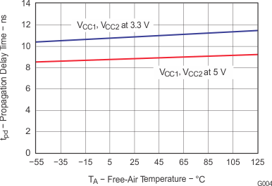
| tPLH, tPHL | Propagation delay time | See Figure 6. | 9 | 14 | ns | |
| PWD(1) | Pulse width distortion |tPHL – tPLH| | 0.3 | 3.7 | ns | ||
| tsk(pp) | Part-to-part skew time | 4.9 | ns | |||
| tsk(o) | Channel-to-channel output skew time | 3.6 | ns | |||
| tr | Output signal rise time | See Figure 6. | 1 | ns | ||
| tf | Output signal fall time | 1 | ns | |||
| tfs | Fail-safe output delay time from input power loss | See Figure 7. | 6 | μs | ||
(1) Also known as pulse skew.
6.11 Switching Characteristics: VCC1 at 5 V ±5%, VCC2 at 3.3 V ±5%
TA = –40°C to 125°C for ISO7420M, TA = –40°C to 105°C for ISO742x| PARAMETER | TEST CONDITIONS | MIN | TYP | MAX | UNIT | |
|---|---|---|---|---|---|---|
| tPLH, tPHL | Propagation delay time | See Figure 6. | 10 | 17 | ns | |
| PWD(1) | Pulse width distortion |tPHL – tPLH| | 0.5 | 5.6 | ns | ||
| tsk(pp) | Part-to-part skew time | 6.3 | ns | |||
| tsk(o) | Channel-to-channel output skew time | 4 | ns | |||
| tr | Output signal rise time | See Figure 6. | 2 | ns | ||
| tf | Output signal fall time | 2 | ns | |||
| tfs | Fail-safe output delay time from input power loss | See Figure 7. | 6 | μs | ||
(1) Also known as pulse skew.
6.12 Switching Characteristics: VCC1 at 3.3 V ±5%, VCC2 at 5 V ±5%
TA = –40°C to 125°C for ISO7420M, TA = –40°C to 105°C for ISO742x| PARAMETER | TEST CONDITIONS | MIN | TYP | MAX | UNIT | |
|---|---|---|---|---|---|---|
| tPLH, tPHL | Propagation delay time | See Figure 6. | 10 | 17 | ns | |
| PWD(1) | Pulse width distortion |tPHL – tPLH| | 0.5 | 4 | ns | ||
| tsk(pp) | Part-to-part skew time | 8.5 | ns | |||
| tsk(o) | Channel-to-channel output skew time | 4 | ns | |||
| tr | Output signal rise time | See Figure 6. | 2 | ns | ||
| tf | Output signal fall time | 2 | ns | |||
| tfs | Fail-safe output delay time from input power loss | See Figure 7. | 6 | μs | ||
(1) Also known as pulse skew.
6.13 Switching Characteristics: VCC1 and VCC2 at 3.3 V ±5%
TA = –40°C to 125°C for ISO7420M, TA = –40°C to 105°C for ISO742x| PARAMETER | TEST CONDITIONS | MIN | TYP | MAX | UNIT | |
|---|---|---|---|---|---|---|
| tPLH, tPHL | Propagation delay time | See Figure 6. | 12 | 20 | ns | |
| PWD(1) | Pulse width distortion |tPHL – tPLH| | 1 | 5 | ns | ||
| tsk(pp) | Part-to-part skew time | 6.8 | ns | |||
| tsk(o) | Channel-to-channel output skew time | 5.5 | ns | |||
| tr | Output signal rise time | See Figure 6. | 2 | ns | ||
| tf | Output signal fall time | 2 | ns | |||
| tfs | Fail-safe output delay time from input power loss | See Figure 7. | 6 | μs | ||
(1) Also known as pulse skew.
6.14 Typical Characteristics
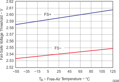 Figure 3. Fail-Safe Voltage Threshold vs Free-Air Temperature
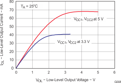 Figure 5. Low-Level Output Current vs Low-Level Output Voltage
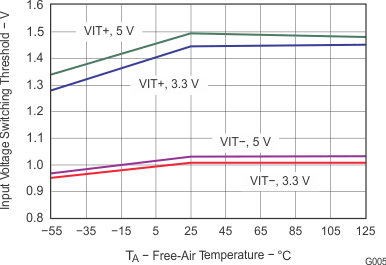 Figure 2. Input Voltage Switching Threshold vs Free-Air Temperature
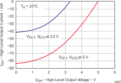 Figure 4. High-Level Output Current vs High-Level Output Voltage
