SWRS283A June 2022 – November 2022 IWR6243
PRODUCTION DATA
- 1 Features
- 2 Applications
- 3 Description
- 4 Functional Block Diagram
- 5 Revision History
- 6 Device Comparison
- 7 Terminal Configuration and Functions
-
8 Specifications
- 8.1 Absolute Maximum Ratings
- 8.2 ESD Ratings
- 8.3 Power-On Hours (POH)
- 8.4 Recommended Operating Conditions
- 8.5 Power Supply Specifications
- 8.6 Power Consumption Summary
- 8.7 RF Specification
- 8.8 Thermal Resistance Characteristics for FCBGA Package [ABL0161]
- 8.9
Timing and Switching Characteristics
- 8.9.1 Power Supply Sequencing and Reset Timing
- 8.9.2 Synchronized Frame Triggering
- 8.9.3 Input Clocks and Oscillators
- 8.9.4 Multibuffered / Standard Serial Peripheral Interface (MibSPI)
- 8.9.5 Inter-Integrated Circuit Interface (I2C)
- 8.9.6 LVDS Interface Configuration
- 8.9.7 General-Purpose Input/Output
- 8.9.8 Camera Serial Interface (CSI2)
- 9 Detailed Description
- 10Monitoring and Diagnostic Mechanisms
- 11Applications, Implementation, and Layout
- 12Device and Documentation Support
- 13Mechanical, Packaging, and Orderable Information
パッケージ・オプション
デバイスごとのパッケージ図は、PDF版データシートをご参照ください。
メカニカル・データ(パッケージ|ピン)
- ABL|161
サーマルパッド・メカニカル・データ
発注情報
8.7 RF Specification
over recommended operating conditions and with run time calibrations enabled
(unless otherwise noted)
| PARAMETER | MIN | TYP | MAX | UNIT | ||
|---|---|---|---|---|---|---|
| Receiver | Noise figure | 10 | dB | |||
| 1-dB compression point (Out Of Band)#T4362547-134 | –12 | dBm | ||||
| Conversion gain at 48db gain setting | 47 | dB | ||||
| Gain range | 18 | dB | ||||
| Gain step size | 2 | dB | ||||
| IF bandwidth#X3038 | 20 | MHz | ||||
| ADC sampling rate (Real/ PseudoReal/ Complex 2x) |
45 | Msps | ||||
| ADC sampling rate (Complex 1x) |
22.5 | Msps | ||||
| ADC resolution | 12 | Bits | ||||
| Idle Channel Spurs | –95 | dBFS | ||||
| Transmitter | Output power | 11.7 | dBm | |||
| Phase shifter accuracy | -11.25 | +16.875 | ° | |||
| Power backoff range | 26 | dB | ||||
| Clock subsystem | Frequency range | 57 | 64 | GHz | ||
| Ramp rate | 250 | MHz/µs | ||||
| Phase noise at 1-MHz offset | –93 | dBc/Hz | ||||
| 20 GHz SYNC OUT signal (FM_CW_CLKOUT and FM_CW_SYNCOUT) | Frequency range | 19 | 21.33 | GHz | ||
| Output power at the pin | 7.5 | dBm | ||||
| Return loss | –8 | dB | ||||
|
Impedance |
50 |
Ω | ||||
| 20 GHz SYNC IN signal (FM_CW_SYNCIN) | Frequency range | 19 | 21.33 | GHz | ||
| Input power at the pin | -3 | 3#GUID-E4C1CB6F-C34C-4099-AE7A-087C157B82BE | dBm | |||
| Return loss | –8 | dB | ||||
| Impedance | 50 | Ω | ||||
(1) 1-dB Compression Point (Out Of Band) is measured by feeding a
continuous wave tone below the lowest HPF cut-off frequency (10 kHz).
(2) The analog IF stages include high-pass filtering, with two independently
configurable first-order high-pass corner frequencies. The set of available HPF corners is
summarized as follows:
The filtering performed by the digital baseband chain is targeted to provide:
| Available HPF Corner Frequencies (kHz) | |
| HPF1 | HPF2 |
| 175,235,350,700 | 350, 700, 1400, 2800 |
- Less than ±0.5 dB pass-band ripple/droop, and
- Better than 60 dB anti-aliasing attenuation for any frequency that can alias back into the pass-band.
(3) The device can tolerate upto 6dBm at temperatures
below 70°C TJ.
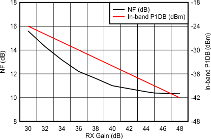
#T4362547-148 shows variations of noise figure and in-band P1dB parameters with respect to receiver gain programmed.
 Figure 8-1 Noise Figure, In-band P1dB vs Receiver
Gain