JAJSQU8 July   2023 IWRL1432

ADVANCE INFORMATION  

  1.   1
  2. 特長
  3. アプリケーション
  4. 概要
  5. 機能ブロック図
  6. Revision History
  7. Device Comparison
    1. 6.1 Related Products
  8. Terminal Configurations and Functions
    1. 7.1 Pin Diagrams
    2. 7.2 Signal Descriptions
      1.      12
      2.      13
      3.      14
      4.      15
      5.      16
      6.      17
      7.      18
      8.      19
      9.      20
      10.      21
      11.      22
      12.      23
      13.      24
      14.      25
      15.      26
      16.      27
      17.      28
    3.     29
  9. Specifications
    1. 8.1  Absolute Maximum Ratings
    2. 8.2  ESD Ratings
    3. 8.3  Power-On Hours (POH)
    4. 8.4  Recommended Operating Conditions
    5. 8.5  Power Supply Specifications
      1. 8.5.1 Power Optimized 3.3V I/O Topology
      2. 8.5.2 BOM Optimized 3.3V I/O Topology
      3. 8.5.3 Power Optimized 1.8V I/O Topology
      4. 8.5.4 BOM Optimized 1.8V I/O Topology
      5. 8.5.5 System Topologies
        1. 8.5.5.1 Power Topologies
          1. 8.5.5.1.1 BOM Optimized Mode
          2. 8.5.5.1.2 Power Optimized Mode
      6. 8.5.6 Noise and Ripple Specifications
    6. 8.6  Power Save Modes
      1. 8.6.1 Typical Power Consumption Numbers
    7. 8.7  Peak Current Requirement per Voltage Rail
    8. 8.8  RF Specification
    9. 8.9  Supported DFE Features
    10. 8.10 CPU Specifications
    11. 8.11 Thermal Resistance Characteristics
    12. 8.12 Timing and Switching Characteristics
      1. 8.12.1  Power Supply Sequencing and Reset Timing
      2. 8.12.2  Synchronized Frame Triggering
      3. 8.12.3  Input Clocks and Oscillators
        1. 8.12.3.1 Clock Specifications
      4. 8.12.4  MultiChannel buffered / Standard Serial Peripheral Interface (McSPI)
        1. 8.12.4.1 McSPI Features
        2. 8.12.4.2 SPI Timing Conditions
        3. 8.12.4.3 SPI—Controller Mode
          1. 8.12.4.3.1 Timing and Switching Requirements for SPI - Controller Mode
          2. 8.12.4.3.2 Timing and Switching Characteristics for SPI Output Timings—Controller Mode
        4. 8.12.4.4 SPI—Peripheral Mode
          1. 8.12.4.4.1 Timing and Switching Requirements for SPI - Peripheral Mode
          2. 8.12.4.4.2 Timing and Switching Characteristics for SPI Output Timings—Secondary Mode
      5. 8.12.5  RDIF Interface Configuration
        1. 8.12.5.1 RDIF Interface Timings
        2. 8.12.5.2 RDIF Data Format
      6. 8.12.6  General-Purpose Input/Output
        1. 8.12.6.1 Switching Characteristics for Output Timing versus Load Capacitance (CL)
      7. 8.12.7  Controller Area Network - Flexible Data-rate (CAN-FD)
        1. 8.12.7.1 Dynamic Characteristics for the CANx TX and RX Pins
      8. 8.12.8  Serial Communication Interface (SCI)
        1. 8.12.8.1 SCI Timing Requirements
      9. 8.12.9  Inter-Integrated Circuit Interface (I2C)
        1. 8.12.9.1 I2C Timing Requirements
      10. 8.12.10 Quad Serial Peripheral Interface (QSPI)
        1. 8.12.10.1 QSPI Timing Conditions
        2. 8.12.10.2 Timing Requirements for QSPI Input (Read) Timings
        3. 8.12.10.3 QSPI Switching Characteristics
      11. 8.12.11 JTAG Interface
        1. 8.12.11.1 JTAG Timing Conditions
        2. 8.12.11.2 Timing Requirements for IEEE 1149.1 JTAG
        3. 8.12.11.3 Switching Characteristics Over Recommended Operating Conditions for IEEE 1149.1 JTAG
  10. Detailed Description
    1. 9.1 Overview
    2. 9.2 機能ブロック図
    3. 9.3 Subsystems
      1. 9.3.1 RF and Analog Subsystem
      2. 9.3.2 Clock Subsystem
      3. 9.3.3 Transmit Subsystem
      4. 9.3.4 Receive Subsystem
      5. 9.3.5 Processor Subsystem
      6. 9.3.6 Host Interface
      7. 9.3.7 Main Subsystem Cortex-M4F
      8. 9.3.8 Hardware Accelerator (HWA1.2) Features
        1. 9.3.8.1 Hardware Accelerator Feature Differences Between HWA1.1 and HWA1.2
    4. 9.4 Other Subsystems
      1. 9.4.1 GPADC Channels (Service) for User Application
      2. 9.4.2 GPADC Parameters
    5. 9.5 Memory Partitioning Options
    6. 9.6 Boot Modes
  11. 10Applications, Implementation, and Layout
    1. 10.1 Application Information
    2. 10.2 Reference Schematic
  12. 11Device and Documentation Support
    1. 11.1 Device Nomenclature
    2. 11.2 Tools and Software
    3. 11.3 Documentation Support
    4. 11.4 Support Resources
    5. 11.5 Trademarks
    6. 11.6 Electrostatic Discharge Caution
    7. 11.7 Glossary
  13. 12Mechanical, Packaging, and Orderable Information

パッケージ・オプション

メカニカル・データ(パッケージ|ピン)
  • AMF|102
サーマルパッド・メカニカル・データ
発注情報
BOM Optimized Mode

In this mode the device can be powered using one 1.8V regulator OR using a 3.3V and a 1.8V regulator mode. The choice of one rail vs two rails is dependent on the IO voltages needed.
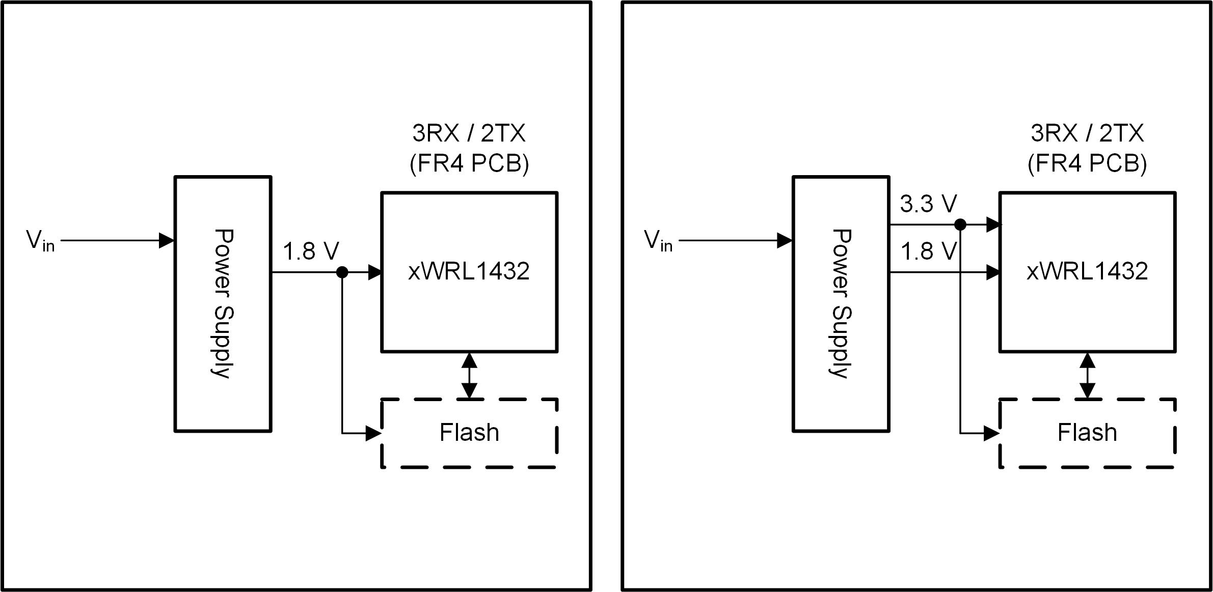
GUID-2250EF86-58F3-46C0-BCAD-AE90AE642C5E-low.jpg Figure 8-2 BOM Optimized Mode Power Management (Left: 1.8V I/O Topology, Right: 3.3V I/O Topology)