SNOSCZ8 April 2016 LDC1612-Q1 , LDC1614-Q1
PRODUCTION DATA.
- 1 Features
- 2 Applications
- 3 Description
- 4 Revision History
- 5 Description Continued
- 6 Pin Configuration and Functions
- 7 Specifications
-
8 Detailed Description
- 8.1 Overview
- 8.2 Functional Block Diagram
- 8.3 Feature Description
- 8.4 Device Functional Modes
- 8.5 Programming
- 8.6
Register Maps
- 8.6.1 Register List
- 8.6.2 Address 0x00, DATA_MSB_CH0
- 8.6.3 Address 0x01, DATA_LSB_CH0
- 8.6.4 Address 0x02, DATA_MSB_CH1
- 8.6.5 Address 0x03, DATA_LSB_CH1
- 8.6.6 Address 0x04, DATA_MSB_CH2 (LDC1614 only)
- 8.6.7 Address 0x05, DATA_LSB_CH2 (LDC1614 only)
- 8.6.8 Address 0x06, DATA_MSB_CH3 (LDC1614 only)
- 8.6.9 Address 0x07, DATA_LSB_CH3 (LDC1614 only)
- 8.6.10 Address 0x08, RCOUNT_CH0
- 8.6.11 Address 0x09, RCOUNT_CH1
- 8.6.12 Address 0x0A, RCOUNT_CH2 (LDC1614 only)
- 8.6.13 Address 0x0B, RCOUNT_CH3 (LDC1614 only)
- 8.6.14 Address 0x0C, OFFSET_CH0
- 8.6.15 Address 0x0D, OFFSET_CH1
- 8.6.16 Address 0x0E, OFFSET_CH2 (LDC1614 only)
- 8.6.17 Address 0x0F, OFFSET_CH3 (LDC1614 only)
- 8.6.18 Address 0x10, SETTLECOUNT_CH0
- 8.6.19 Address 0x11, SETTLECOUNT_CH1
- 8.6.20 Address 0x12, SETTLECOUNT_CH2 (LDC1614 only)
- 8.6.21 Address 0x13, SETTLECOUNT_CH3 (LDC1614 only)
- 8.6.22 Address 0x14, CLOCK_DIVIDERS_CH0
- 8.6.23 Address 0x15, CLOCK_DIVIDERS_CH1
- 8.6.24 Address 0x16, CLOCK_DIVIDERS_CH2 (LDC1614 only)
- 8.6.25 Address 0x17, CLOCK_DIVIDERS_CH3 (LDC1614 only)
- 8.6.26 Address 0x18, STATUS
- 8.6.27 Address 0x19, ERROR_CONFIG
- 8.6.28 Address 0x1A, CONFIG
- 8.6.29 Address 0x1B, MUX_CONFIG
- 8.6.30 Address 0x1C, RESET_DEV
- 8.6.31 Address 0x1E, DRIVE_CURRENT_CH0
- 8.6.32 Address 0x1F, DRIVE_CURRENT_CH1
- 8.6.33 Address 0x20, DRIVE_CURRENT_CH2 (LDC1614 only)
- 8.6.34 Address 0x21, DRIVE_CURRENT_CH3 (LDC1614 only)
- 8.6.35 Address 0x7E, MANUFACTURER_ID
- 8.6.36 Address 0x7F, DEVICE_ID
- 9 Application and Implementation
- 10Power Supply Recommendations
- 11Layout
- 12Device and Documentation Support
- 13Mechanical, Packaging, and Orderable Information
7 Specifications
7.1 Absolute Maximum Ratings
(1)| MIN | MAX | UNIT | ||
|---|---|---|---|---|
| VDD | Supply Voltage | 5 | V | |
| Vi | Voltage on any pin | –0.3 | VDD+0.3 | V |
| IA | Input current on any INx pin | –8 | 8 | mA |
| ID | Input current on any Digital pin | –5 | 5 | mA |
| Tj | Junction Temperature | –55 | 150 | °C |
| Tstg | Storage temperature range | –65 | 150 | °C |
(1) Stresses beyond those listed under Absolute Maximum Ratings may cause permanent damage to the device. These are stress ratings only, which do not imply functional operation of the device at these or any other conditions beyond those indicated under Recommended Operating Conditions. Exposure to absolute-maximum-rated conditions for extended periods may affect device reliability.
7.2 ESD Ratings
| VALUE | UNIT | |||
|---|---|---|---|---|
| V(ESD) | Electrostatic discharge | Human-body model (HBM), per AEC Q100-002(1) | ±2000 | V |
| Charged-device model (CDM), per AEC Q100-011 | ±750 | |||
(1) AEC Q100-002 indicates that HBM stressing shall be in accordance with the ANSI/ESDA/JEDEC JS-001 specification.
7.3 Recommended Operating Conditions
Unless otherwise specified, all limits ensured for TA = 25°C, VDD = 3.3 V| MIN | NOM | MAX | UNIT | ||
|---|---|---|---|---|---|
| VDD | Supply Voltage | 2.7 | 3.6 | V | |
| TA | Operating Temperature | –40 | 125 | °C | |
7.4 Thermal Information
| THERMAL METRIC(1) | LDC1612 | LDC1614 | UNIT | |
|---|---|---|---|---|
| DNT (WSON) | RGH (WQFN) | |||
| 12 PINS | 16 PINS | |||
| RθJA | Junction-to-ambient thermal resistance | 36.7 | 35.6 | °C/W |
| RθJC(top) | Junction-to-case (top) thermal resistance | 36.2 | 36.2 | °C/W |
| RθJB | Junction-to-board thermal resistance | 14 | 13.4 | °C/W |
| ψJT | Junction-to-top characterization parameter | 0.4 | 0.4 | °C/W |
| ψJB | Junction-to-board characterization parameter | 14.2 | 13.4 | °C/W |
| RθJC(bot) | Junction-to-case (bottom) thermal resistance | 3.5 | 3.5 | °C/W |
(1) For more information about traditional and new thermal metrics, see the Semiconductor and IC Package Thermal Metrics application report, SPRA953.
7.5 Electrical Characteristics (4)
Unless otherwise specified, all limits ensured for TA = 25°C, VDD = 3.3 V| PARAMETER | TEST CONDITIONS(3) | MIN(5) | TYP(6) | MAX(5) | UNIT | |
|---|---|---|---|---|---|---|
| POWER | ||||||
| VDD | Supply Voltage | TA = –40°C to +125°C | 2.7 | 3.6 | V | |
| IDD | Supply Current (not including sensor current)(1) | CLKIN = 10MHz (2) | 2.1 | mA | ||
| IDDSL | Sleep Mode Supply Current(1) | 35 | 60 | µA | ||
| ISD | Shutdown Mode Supply Current(1) | 0.2 | 1 | µA | ||
| SENSOR | ||||||
| ISENSORMAX | Sensor Maximum Current drive | HIGH_CURRENT_DRV = b0 DRIVE_CURRENT_CHx = 0xF800 |
1.5 | mA | ||
| RP | Sensor RP | 1 | 100 | kΩ | ||
| IHDSENSORMAX | High current sensor drive mode: Sensor Maximum Current | HIGH_CURRENT_DRV = b1 DRIVE_CURRENT_CH0 = 0xF800 Channel 0 only |
6 | mA | ||
| RP_HD_MIN | Minimum sensor RP | 250 | Ω | |||
| fSENSOR | Sensor Resonance Frequency | TA = –40°C to +125°C | 0.001 | 10 | MHz | |
| VSENSORMAX | Maximum oscillation amplitude (peak) | 1.8 | V | |||
| NBITS | Number of bits | 28 | bits | |||
| fCS | Maximum Channel Sample Rate | single active channel continuous conversion, SCL=400kHz | 4.08 | kSPS | ||
| CIN | Sensor Pin input capacitance | 4 | pF | |||
| MASTER CLOCK | ||||||
| fCLKIN | External Master Clock Input Frequency (CLKIN) | TA = –40°C to +125°C | 2 | 40 | MHz | |
| CLKINDUTY_MIN | External Master Clock minimum acceptable duty cycle (CLKIN) | 40% | ||||
| CLKINDUTY_MAX | External Master Clock maximum acceptable duty cycle (CLKIN) | 60% | ||||
| VCLKIN_LO | CLKIN low voltage threshold | 0.3ˣVDD | V | |||
| VCLKIN_HI | CLKIN high voltage threshold | 0.7ˣVDD | V | |||
| fINTCLK | Internal Master Clock Frequency range | 35 | 43.4 | 55 | MHz | |
| TCf_int_μ | Internal Master Clock Temperature Coefficient mean | –13 | ppm/°C | |||
(1) I2C read/write communication and pullup resistors current through SCL, SDA not included.
(2) Sensor inductor: 2 layer, 32 turns/layer, 14mm diameter, PCB inductor with L=19.4 µH, RP=5.7 kΩ at 2MHz Sensor capacitor: 330 pF 1% COG/NP0 Target: Aluminum, 1.5mm thickness Channel = Channel 0 (continuous mode) CLKIN = 40 MHz, CHx_FIN_DIVIDER = b0000, CHx_FREF_DIVIDER = b00 0000 0001 CH0_RCOUNT = 0xFFFF, SETTLECOUNT_CH0 = 0x0100 RP_OVERRIDE = b1, AUTO_AMP_DIS = b1, DRIVE_CURRENT_CH0 = 0x9800
(3) Register values are represented as either binary (b is the prefix to the digits), or hexadecimal (0x is the prefix to the digits). Decimal values have no prefix.
(4) Electrical Characteristics Table values apply only for factory testing conditions at the temperature indicated. Factory testing conditions result in very limited self-heating of the device such that TJ = TA. Absolute Maximum Ratings indicate junction temperature limits beyond which the device may be permanently degraded, either mechanically or electrically.
(5) Limits are ensured by testing, design, or statistical analysis at 25°C. Limits over the operating temperature range are ensured through correlations using statistical quality control (SQC) method.
(6) Typical values represent the most likely parametric norm as determined at the time of characterization. Actual typical values may vary over time and also depend on the application and configuration. The typical values are not tested and are not ensured on shipped production material.
7.6 Timing Characteristics
| MIN | NOM | MAX | UNIT | ||
|---|---|---|---|---|---|
| tWAKEUP | Wake-up Time from SD high-low transition to I2C readback | 2 | ms | ||
| tWD-TIMEOUT | Sensor recovery time (after watchdog timeout) | 5.2 | ms | ||
7.7 Switching Characteristics - I2C
Unless otherwise specified, all limits ensured for TA = 25°C, VDD = 3.3 V| PARAMETER | TEST CONDITIONS | MIN | TYP | MAX | UNIT | |
|---|---|---|---|---|---|---|
| VOLTAGE LEVELS | ||||||
| VIH | Input High Voltage | 0.7ˣVDD | V | |||
| VIL | Input Low Voltage | 0.3ˣVDD | V | |||
| VOL | Output Low Voltage (3mA sink current) | 0.4 | V | |||
| HYS | Hysteresis | 0.1ˣVDD | V | |||
| I2C TIMING CHARACTERISTICS | ||||||
| fSCL | Clock Frequency | 10 | 400 | kHz | ||
| tLOW | Clock Low Time | 1.3 | μs | |||
| tHIGH | Clock High Time | 0.6 | μs | |||
| tHD;STA | Hold Time (repeated) START condition | After this period, the first clock pulse is generated | 0.6 | μs | ||
| tSU;STA | Set-up time for a repeated START condition | 0.6 | μs | |||
| tHD;DAT | Data hold time | 0 | μs | |||
| tSU;DAT | Data setup time | 100 | ns | |||
| tSU;STO | Set-up time for STOP condition | 0.6 | μs | |||
| tBUF | Bus free time between a STOP and START condition | 1.3 | μs | |||
| tVD;DAT | Data valid time | 0.9 | μs | |||
| tVD;ACK | Data valid acknowledge time | 0.9 | μs | |||
| tSP | Pulse width of spikes that must be suppressed by the input filter(1) | 50 | ns | |||
(1) This parameter is specified by design and/or characterization and is not tested in production.
 Figure 1. I2C Timing
7.8 Typical Characteristics
Common test conditions (unless specified otherwise): Sensor inductor: 2 layer, 32 turns/layer, 14 mm diameter, PCB inductor with L=19.4 µH, RP=5.7 kΩ at 2 MHz; Sensor capacitor: 330 pF 1% COG/NP0; Target: Aluminum, 1.5mm thickness; Channel = Channel 0 (continuous mode); CLKIN = 40 MHz, CHx_FIN_DIVIDER = 0x1, CHx_FREF_DIVIDER = 0x001, CH0_RCOUNT = 0xFFFF, SETTLECOUNT_CH0 = 0x0100, RP_OVERRIDE = 1, AUTO_AMP_DIS = 1, DRIVE_CURRENT_CH0 = 0x9800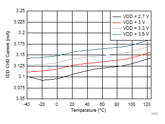
| Includes 1.57 mA sensor coil current | ||
| –40°C to +125°C |
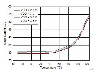
| –40°C to +125°C |
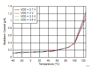
| –40°C to +125°C |
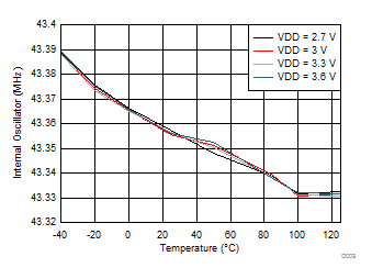
| –40°C to +125°C | ||
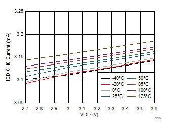
| Includes 1.57 mA sensor coil current | ||
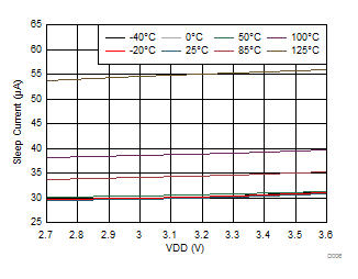
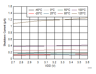
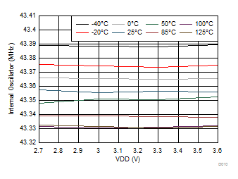
| Data based on 1 unit | ||