JAJSL91 april 2021 LM117QML-SP
PRODUCTION DATA
- 1
- 1 特長
- 2 アプリケーション
- 3 概要
- 4 Revision History
- 5 Device Comparison Table
- 6 Pin Configurations and Functions
-
7 Specifications
- 7.1 Absolute Maximum Ratings
- 7.2 ESD Ratings
- 7.3 Recommended Operating Conditions
- 7.4 Thermal Information
- 7.5 Electrical Characteristics: 0.5–A IOUT Devices (LM117H, LM117GW)
- 7.6 Parameter Drift: 0.5–A IOUT Devices (LM117H, LM117GW)
- 7.7 Electrical Characteristics: 1.5–A IOUT Devices (LM117K)
- 7.8 Parameter Drift: 1.5–A IOUT Devices (LM117K)
- 7.9 Quality Conformance Inspection
- 7.10 Typical Characteristics
- 8 Detailed Description
- 9 Application and Implementation
- 10Power Supply Recommendations
- 11Layout
- 12Device and Documentation Support
パッケージ・オプション
メカニカル・データ(パッケージ|ピン)
サーマルパッド・メカニカル・データ
発注情報
6 Pin Configurations and Functions
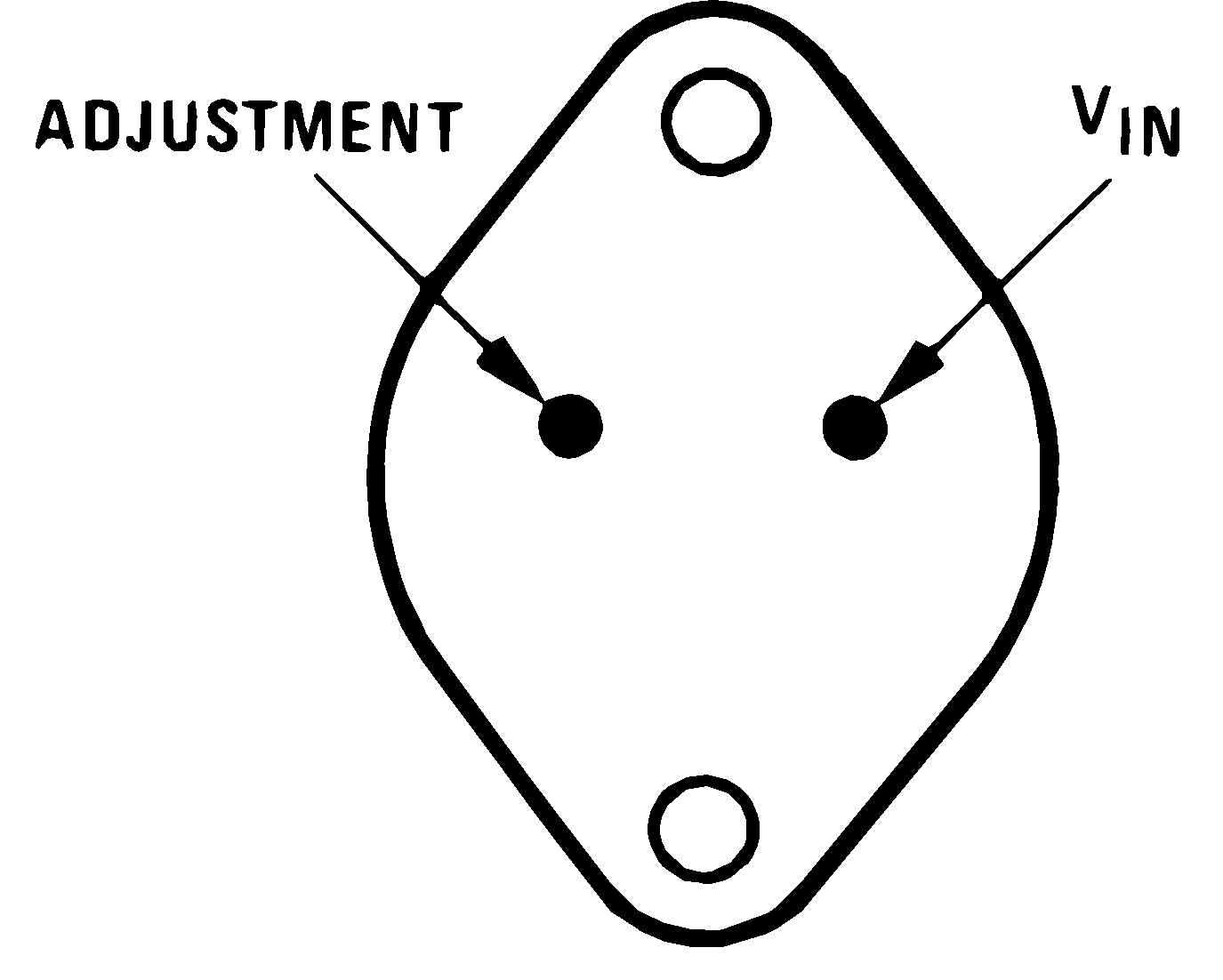
 Figure 6-1 LM117K K Package
2-Pin TO-3 (Metal Can)
Bottom View
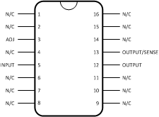
 Figure 6-3 LM117GW NAC Package
16-Pin CFP SOIC
Top View
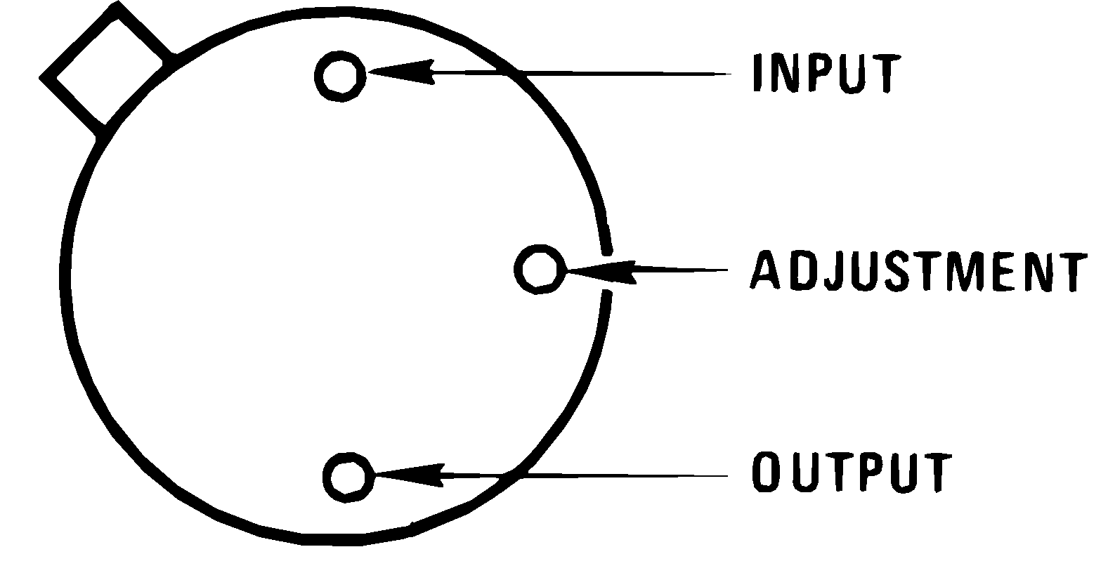
 Figure 6-2 LM117H, LM117NDT NDT
Package
Figure 6-2 LM117H, LM117NDT NDT
Package3-Pin TO-39 (Metal Can)
Bottom View
Table 6-1 Pin Functions
| PIN | I/O | DESCRIPTION | |||
|---|---|---|---|---|---|
| NAME | TO-3 | TO-39 | CFP SOIC | ||
| ADJ | 1 | 2 | 3 | — | Adjust pin |
| VIN | 2 | 1 | 5 | I | Input voltage pin for the regulator |
| VOUT | CASE | 3, CASE | 12 | O | Output voltage pin for the regulator |
| OUTPUT/SENSE | — | — | 13 | — | Used to sense the output voltage. Must be connected to VOUT for proper operation. |
| N/C | — | — | 1, 2, 4, 6, 7, 8, 9, 10, 11, 14, 15, 16 | — | No connection. These pins have no internal connections and may be grounded or left floating. They may also be connected to the board heatsink and used for thermal dissipation. |