SNOSBI2C June 1999 – September 2015 LM231 , LM331
PRODUCTION DATA.
- 1 Features
- 2 Applications
- 3 Description
- 4 Revision History
- 5 Description continued
- 6 Pin Configuration and Functions
- 7 Specifications
- 8 Detailed Description
- 9 Application and Implementation
- 10Power Supply Recommendations
- 11Layout
- 12Device and Documentation Support
- 13Mechanical, Packaging, and Orderable Information
7 Specifications
7.1 Absolute Maximum Ratings(2)(1)(1)
| MIN | MAX | UNIT | ||
|---|---|---|---|---|
| Supply Voltage, VS | 40 | V | ||
| Output Short Circuit to Ground | Continuous | |||
| Output Short Circuit to VCC | Continuous | |||
| Input Voltage | −0.2 | +VS | V | |
| Lead Temperature (Soldering, 10 sec.) | PDIP | 260 | °C | |
(1) If Military/Aerospace specified devices are required, please contact the TI Sales Office/Distributors for availability and specifications.
(2) Stresses beyond those listed under Absolute Maximum Ratings may cause permanent damage to the device. These are stress ratings only, which do not imply functional operation of the device at these or any other conditions beyond those indicated under Recommended Operating Conditions. Exposure to absolute-maximum-rated conditions for extended periods may affect device reliability.
7.2 ESD Ratings
| VALUE | UNIT | |||
|---|---|---|---|---|
| V(ESD) | Electrostatic discharge | Human body model (HBM), per ANSI/ESDA/JEDEC JS-001(1)(2) | ±500 | V |
(1) JEDEC document JEP155 states that 500-V HBM allows safe manufacturing with a standard ESD control process.
(2) Human body model, 100 pF discharged through a 1.5-kΩ resistor.
7.3 Recommended Operating Conditions
| MIN | MAX | UNIT | ||
|---|---|---|---|---|
| Operating Ambient Temperature | LM231, LM231A | −25 | 85 | °C |
| LM331, LM331A | 0 | 70 | °C | |
| Supply Voltage, VS(1) | 4 | 40 | V | |
(1) All voltages are measured with respect to GND = 0 V, unless otherwise noted.
7.4 Thermal Information
| THERMAL METRIC(1) | LM312, LM331 | UNIT | |
|---|---|---|---|
| P (PDIP) | |||
| 8 PINS | |||
| RθJA | Junction-to-ambient thermal resistance | 100 | °C/W |
(1) For more information about traditional and new thermal metrics, see the Semiconductor and IC Package Thermal Metrics application report, SPRA953.
7.5 Electrical Characteristics
All specifications apply in the circuit of Figure 16, with 4.0 V ≤ VS ≤ 40 V, TA = 25°C, unless otherwise specified.| PARAMETER | TEST CONDITIONS | MIN | TYP | MAX | UNIT | |
|---|---|---|---|---|---|---|
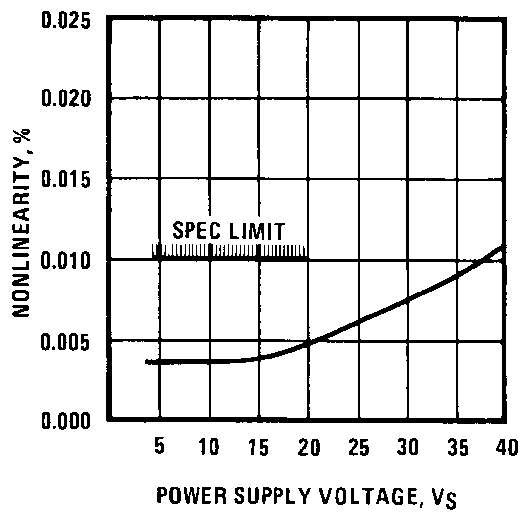
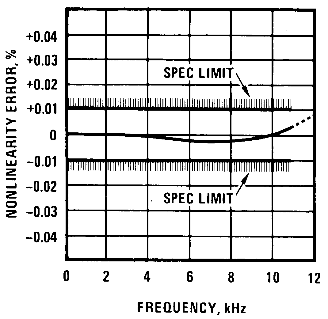
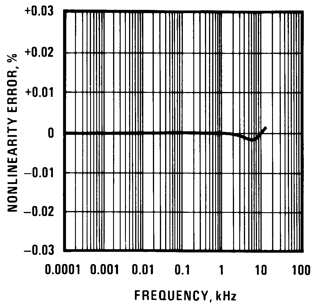
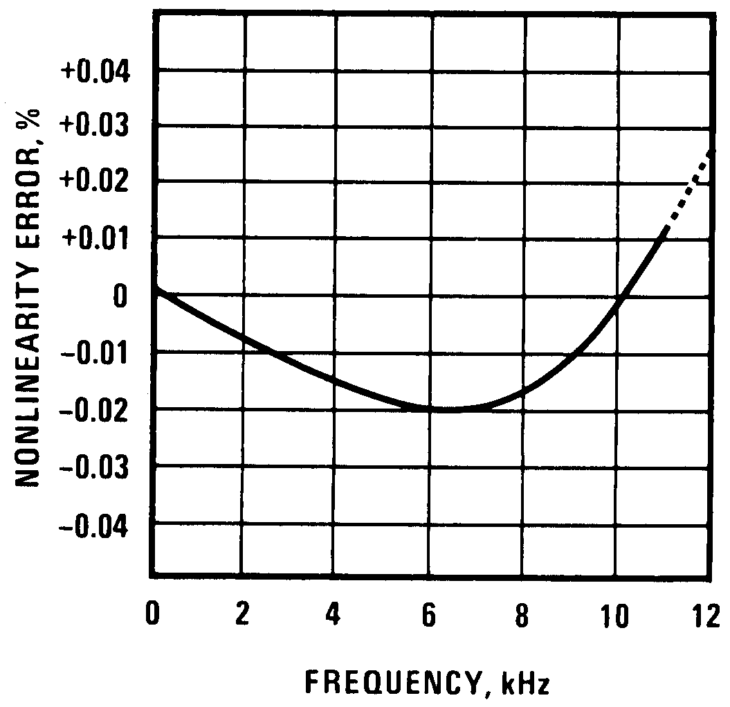
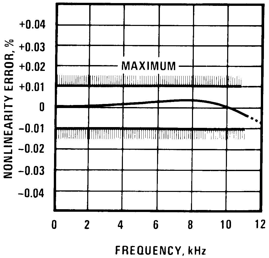
| VFC Non-Linearity (1) | 4.5 V ≤ VS ≤ 20 V | ±0.003 | ±0.01 | % Full-Scale | ||
| TMIN ≤ TA ≤ TMAX | ±0.006 | ±0.02 | % Full-Scale | |||
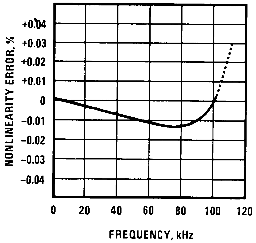
| VFC Non-Linearity in Circuit of Figure 14 | VS = 15 V, f = 10 Hz to 11 kHz | ±0.024 | ±0.14 | %Full-Scale | ||
| Conversion Accuracy Scale Factor (Gain) | LM231, LM231A | VIN = −10 V, RS = 14 kΩ | 0.95 | 1 | 1.05 | kHz/V |
| LM331, LM331A | 0.9 | 1 | 1.1 | kHz/V | ||
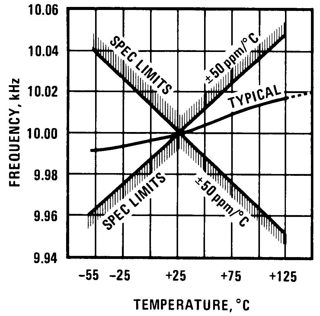
| Temperature Stability of Gain | LMx31 | TMIN ≤ TA ≤ TMAX
4.5 V ≤ VS ≤ 20 V |
±30 | ±150 | ppm/°C | |
| LMx31A | ±20 | ±50 | ppm/°C | |||
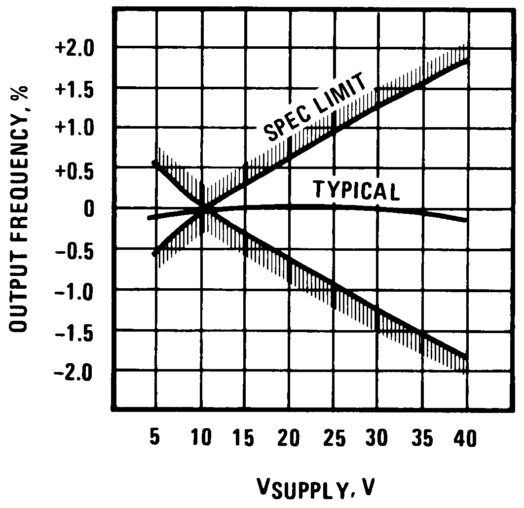
| Change of Gain with VS | 4.5 V ≤ VS ≤ 10 V | 0.01 | 0.1 | %/V | ||
| 10 V ≤ VS ≤ 40 V | 0.006 | 0.06 | %/V | |||
| Rated Full-Scale Frequency | VIN = −10 V | 10.0 | kHz | |||
| Gain Stability vs. Time (1000 Hours) | TMIN ≤ TA ≤ TMAX | ±0.02 | % Full- Scale | |||
| Over Range (Beyond Full-Scale) Frequency | VIN = −11 V | 10% | ||||
| INPUT COMPARATOR | ||||||
| Offset Voltage | ±3 | ±10 | mV | |||
| LM231/LM331 | TMIN ≤ TA ≤ TMAX | ±4 | ±14 | mV | ||
| LM231A/LM331A | TMIN ≤ TA ≤ TMAX | ±3 | ±10 | mV | ||
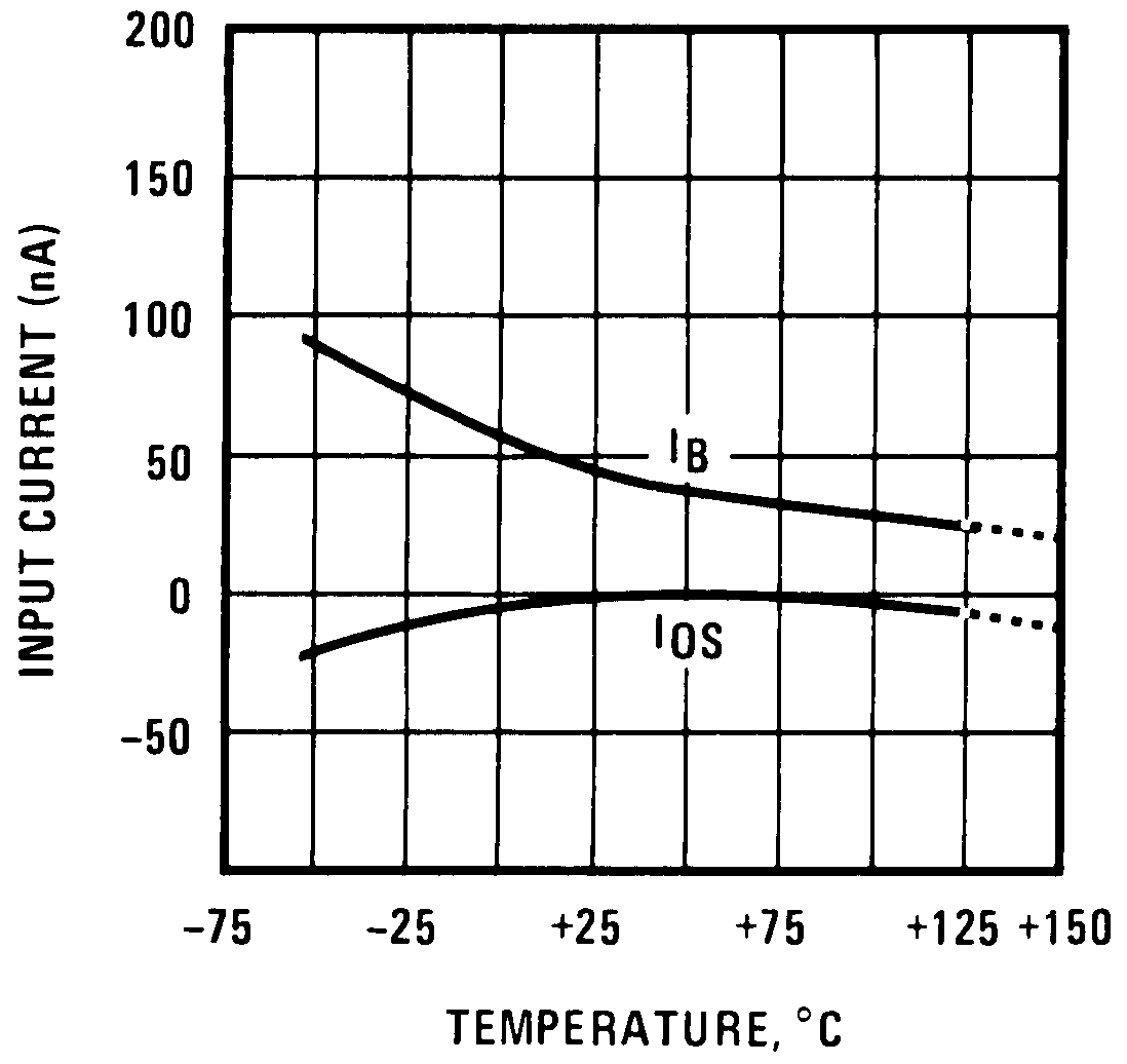
| Bias Current | −80 | −300 | nA | |||
| Offset Current | ±8 | ±100 | nA | |||
| Common-Mode Range | TMIN ≤ TA ≤ TMAX | −0.2 | VCC − 2 | V | ||
| TIMER | ||||||
| Timer Threshold Voltage, Pin 5 | 0.63 × VS | 0.667 × VS | 0.7 × VS | |||
| Input Bias Current, Pin 5 | VS = 15 V | |||||
| All Devices | 0V ≤ VPIN 5 ≤ 9.9 V | ±10 | ±100 | nA | ||
| LM231/LM331 | VPIN 5 = 10 V | 200 | 1000 | nA | ||
| LM231A/LM331A | VPIN 5 = 10 V | 200 | 500 | nA | ||
| VSAT PIN 5 (Reset) | I = 5 mA | 0.22 | 0.5 | V | ||
| CURRENT SOURCE (PIN 1) | ||||||
| Output Current | LM231, LM231A | RS = 14 kΩ, VPIN 1 = 0 | 126 | 135 | 144 | μA |
| LM331, LM331A | 116 | 136 | 156 | μA | ||
| Change with Voltage | 0V ≤ VPIN 1 ≤ 10 V | 0.2 | 1 | μA | ||
| Current Source OFF Leakage | LM231, LM231A, LM331, LM331A | 0.02 | 10 | nA | ||
| All Devices | TA = TMAX | 2 | 50 | nA | ||
| Operating Range of Current (Typical) | (10 to 500) | μA | ||||
| REFERENCE VOLTAGE (PIN 2) | ||||||
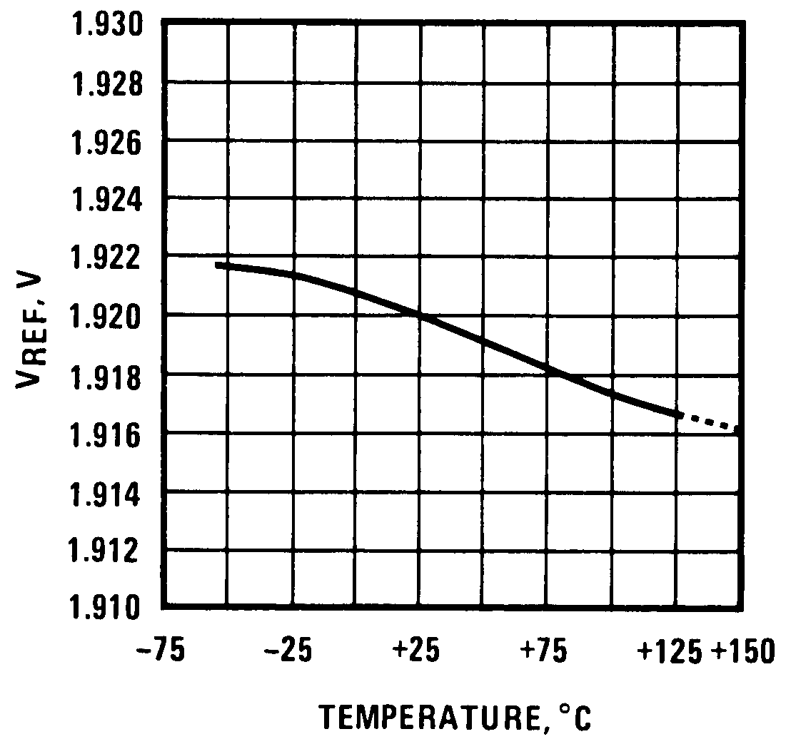
| LM231, LM231A | 1.76 | 1.89 | 2.02 | VDC | ||
| LM331, LM331A | 1.7 | 1.89 | 2.08 | VDC | ||
| Stability vs. Temperature | ±60 | ppm/°C | ||||
| Stability vs. Time, 1000 Hours | ±0.1% | |||||
| LOGIC OUTPUT (PIN 3) | ||||||
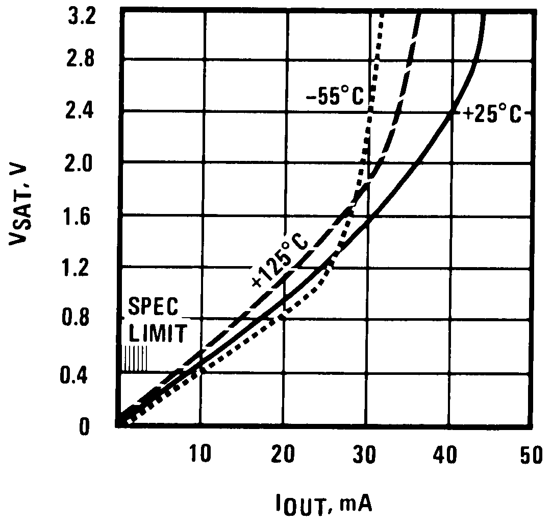
| VSAT | I = 5 mA | 0.15 | 0.5 | V | ||
| I = 3.2 mA (2 TTL Loads), TMIN ≤ TA ≤ TMAX |
0.1 | 0.4 | V | |||
| OFF Leakage | ±0.05 | 1 | μA | |||
| SUPPLY CURRENT | ||||||
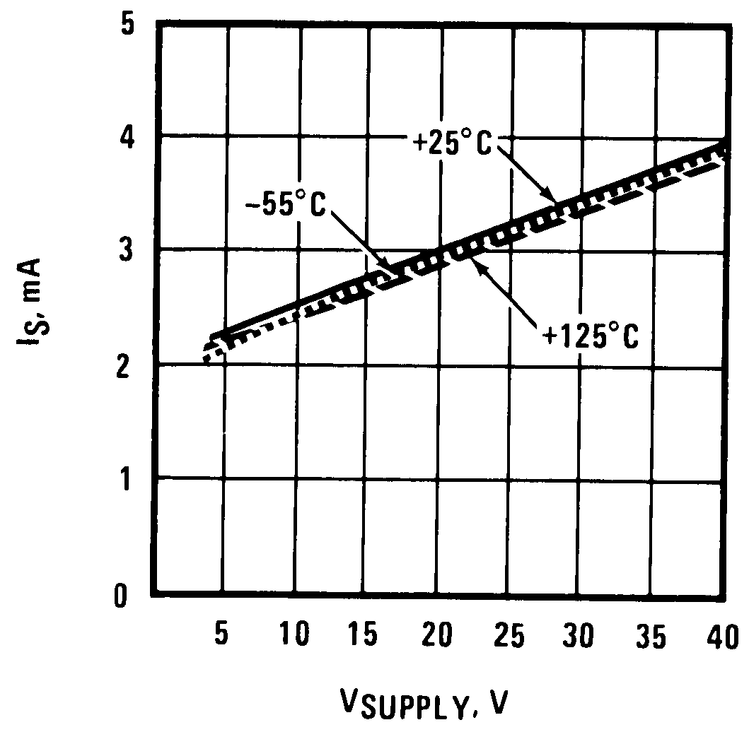
| LM231, LM231A | VS = 5 V | 2 | 3 | 4 | mA | |
| VS = 40 V | 2.5 | 4 | 6 | mA | ||
| LM331, LM331A | VS = 5 V | 1.5 | 3 | 6 | mA | |
| VS = 40 V | 2 | 4 | 8 | mA | ||
(1) Non-linearity is defined as the deviation of fOUT from VIN × (10 kHz/−10 VDC) when the circuit has been trimmed for zero error at 10 Hz and at 10 kHz, over the frequency range 1 Hz to 11 kHz. For the timing capacitor, CT, use NPO ceramic, Teflon®, or polystyrene.
7.6 Dissipation Ratings
| VALUE | UNIT | |||
|---|---|---|---|---|
| Package Dissipation at 25°C(1) | 1.25 | W | ||
(1) The absolute maximum junction temperature (TJmax) for this device is 150°C. The maximum allowable power dissipation is dictated by TJmax, the junction-to-ambient thermal resistance (θJA), and the ambient temperature TA, and can be calculated using the formula PDmax = (TJmax - TA) / θJA. The values for maximum power dissipation will be reached only when the device is operated in a severe fault condition (e.g., when input or output pins are driven beyond the power supply voltages, or the power supply polarity is reversed). Obviously, such conditions should always be avoided.
7.7 Typical Characteristics
(All electrical characteristics apply for the circuit of Figure 16, unless otherwise noted.)