JAJSDG8F July 2011 – March 2018 LM25118
PRODUCTION DATA.
- 1 特長
- 2 アプリケーション
- 3 概要
- 4 改訂履歴
- 5 Pin Configuration and Functions
- 6 Specifications
- 7 Detailed Description
-
8 Application and Implementation
- 8.1 Application Information
- 8.2
Typical Application
- 8.2.1 Design Requirements
- 8.2.2
Detailed Design Procedure
- 8.2.2.1 Custom Design With WEBENCH® Tools
- 8.2.2.2 R7 = RT
- 8.2.2.3 Inductor Selection – L1
- 8.2.2.4 R13 = RSENSE
- 8.2.2.5 C15 = CRAMP
- 8.2.2.6 Inductor Current Limit Calculation
- 8.2.2.7 C9 - C12 = Output Capacitors
- 8.2.2.8 D1
- 8.2.2.9 D4
- 8.2.2.10 C1 – C5 = Input Capacitors
- 8.2.2.11 C20
- 8.2.2.12 C8
- 8.2.2.13 C16 = CSS
- 8.2.2.14 R8, R9
- 8.2.2.15 R1, R3, C21
- 8.2.2.16 R2
- 8.2.2.17 Snubber
- 8.2.2.18 Error Amplifier Configuration
- 8.2.3 Application Curves
- 9 Power Supply Recommendations
- 10Layout
- 11デバイスおよびドキュメントのサポート
- 12メカニカル、パッケージ、および注文情報
パッケージ・オプション
メカニカル・データ(パッケージ|ピン)
- PWP|20
サーマルパッド・メカニカル・データ
- PWP|20
発注情報
7.3.6 Maximum Duty Cycle
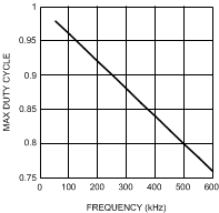
Each conduction cycle of the buck switch is followed by a forced minimum off-time of 400 ns to allow sufficient time for the recirculating diode current to be sampled. This forced off-time limits the maximum duty cycle of the controller. The actual maximum duty cycle will vary with the operating frequency of Equation 7.
where
- f is the oscillator frequency in Hz
 Figure 15. Maximum Duty Cycle vs Frequency
Limiting the maximum duty cycle will limit the maximum boost ratio (VOUT/VIN) while operating in buck-boost mode. For example, from Figure 15, at an operating frequency of 500 kHz, DMAX is 80%. Using the buck-boost transfer function.

with
- D = 80%, solving for VOUT results in
- VOUT = 4 × VIN
With a minimum input voltage of 5 V, the maximum possible output voltage is 20 V at f = 500 kHz. The buck-boost step-up ratio can be increased by reducing the operating frequency which increases the maximum duty cycle.