JAJS852E May   1996  – May 2019 LM2586

PRODUCTION DATA.  

  1. 特長
  2. 代表的なアプリケーション
  3. 概要
    1.     Device Images
      1.      ブロック図
  4. 改訂履歴
  5. 概要(続き)
  6. Pin Configurations
  7. Specifications
    1. 7.1 Absolute Maximum Ratings
    2. 7.2 ESD Ratings
    3. 7.3 Recommended Operating Ratings
    4. 7.4 Thermal Information
    5. 7.5 Electrical Characteristics: 3.3 V
    6. 7.6 Electrical Characteristics: 5 V
    7. 7.7 Electrical Characteristics: 12 V
    8. 7.8 Electrical Characteristics: Adjustable
    9. 7.9 Typical Characteristics
  8. Detailed Description
    1. 8.1 Overview
    2. 8.2 Functional Block Diagram
    3. 8.3 Feature Description
      1. 8.3.1 Flyback Regulator Operation
      2. 8.3.2 Step-Up (Boost) Regulator Operation
      3. 8.3.3 Programming Output Voltage (Selecting R1 And R2)
      4. 8.3.4 Shutdown Control
      5. 8.3.5 Frequency Adjustment
      6. 8.3.6 Frequency Synchronization
  9. Application and Implementation
    1. 9.1 Application Information
    2. 9.2 Typical Applications
      1. 9.2.1 Typical Flyback Regulator Applications
        1. 9.2.1.1 Design Requirements
          1. 9.2.1.1.1 Transformer Selection (T)
          2. 9.2.1.1.2 Transformer Footprints
        2. 9.2.1.2 Detailed Design Procedure
          1. 9.2.1.2.1 Custom Design With WEBENCH® Tools
          2. 9.2.1.2.2 Flyback Regulator Input Capacitors
          3. 9.2.1.2.3 Switch Voltage Limits
          4. 9.2.1.2.4 Output Voltage Limitations
          5. 9.2.1.2.5 Noisy Input Line Condition
          6. 9.2.1.2.6 Stability
      2. 9.2.2 Typical Boost Regulator Applications
        1. 9.2.2.1 Design Requirements
        2. 9.2.2.2 Detailed Design Procedure
    3. 9.3 System Examples
      1. 9.3.1 Test Circuits
  10. 10Layout
    1. 10.1 Layout Guidelines
    2. 10.2 Layout Example
  11. 11Heat Sink/Thermal Considerations
  12. 12デバイスおよびドキュメントのサポート
    1. 12.1 デバイス・サポート
      1. 12.1.1 デベロッパー・ネットワークの製品に関する免責事項
      2. 12.1.2 開発サポート
        1. 12.1.2.1 WEBENCH®ツールによるカスタム設計
    2. 12.2 ドキュメントの更新通知を受け取る方法
    3. 12.3 コミュニティ・リソース
    4. 12.4 商標
    5. 12.5 静電気放電に関する注意事項
    6. 12.6 Glossary
  13. 13メカニカル、パッケージ、および注文情報

パッケージ・オプション

メカニカル・データ(パッケージ|ピン)
サーマルパッド・メカニカル・データ
発注情報

Flyback Regulator Input Capacitors

A flyback regulator draws discontinuous pulses of current from the input supply. Therefore, there are two input capacitors needed in a flyback regulator—one for energy storage and one for filtering (see Figure 48). Both are required due to the inherent operation of a flyback regulator. To keep a stable or constant voltage supply to the LM2586, a storage capacitor (≥100 μF) is required. If the input source is a rectified DC supply and/or the application has a wide temperature range, the required rms current rating of the capacitor might be very large. This means a larger value of capacitance or a higher voltage rating will be needed for the input capacitor. The storage capacitor will also attenuate noise which may interfere with other circuits connected to the same input supply voltage.
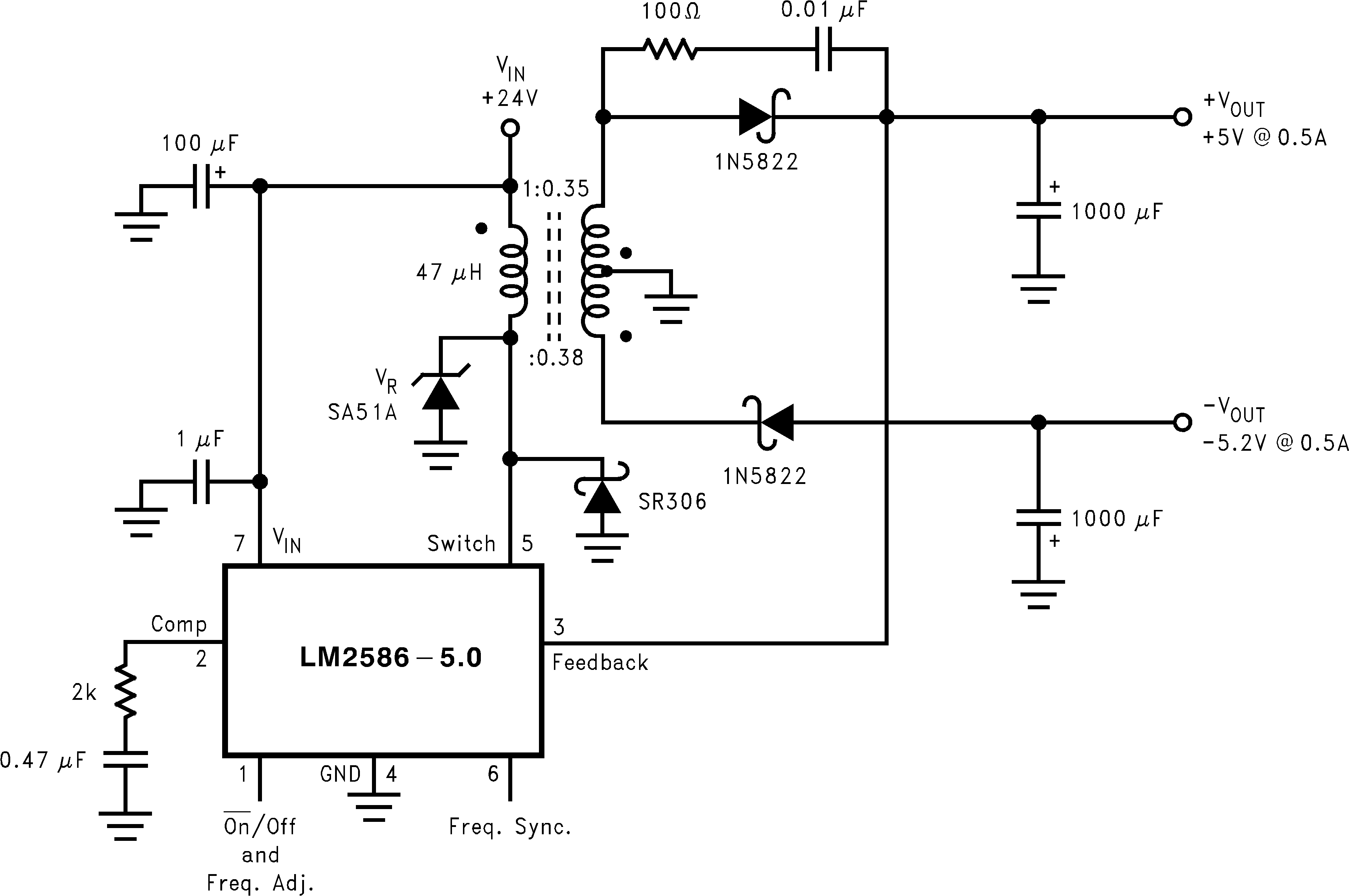
LM2586 01251662.pngFigure 48. Flyback Regulator

In addition, a small bypass capacitor is required due to the noise generated by the input current pulses. To eliminate the noise, insert a 1-μF ceramic capacitor between VIN and ground as close as possible to the device.