JAJSA30G November 2002 – May 2019 LM2733
PRODUCTION DATA.
- 1 特長
- 2 アプリケーション
- 3 概要
- 4 改訂履歴
- 5 Pin Configuration and Functions
- 6 Specifications
- 7 Detailed Description
-
8 Application and Implementation
- 8.1 Application Information
- 8.2
Typical Application
- 8.2.1 Design Requirements
- 8.2.2
Detailed Design Procedure
- 8.2.2.1 Selecting the External Capacitors
- 8.2.2.2 Selecting the Output Capacitor
- 8.2.2.3 Selecting the Input Capacitor
- 8.2.2.4 Feedforward Compensation
- 8.2.2.5 Selecting Diodes
- 8.2.2.6 Setting the Output Voltage
- 8.2.2.7 Switching Frequency
- 8.2.2.8 Duty Cycle
- 8.2.2.9 Inductance Value
- 8.2.2.10 Maximum Switch Current
- 8.2.2.11 Calculating Load Current
- 8.2.2.12 Design Parameters VSW and ISW
- 8.2.2.13 Thermal Considerations
- 8.2.2.14 Minimum Inductance
- 8.2.2.15 Inductor Suppliers
- 8.2.3 Application Curves
- 9 Power Supply Recommendations
- 10Layout
- 11デバイスおよびドキュメントのサポート
- 12メカニカル、パッケージ、および注文情報
8.2.2.14 Minimum Inductance
In some applications where the maximum load current is relatively small, it may be advantageous to use the smallest possible inductance value for cost and size savings. The converter will operate in discontinuous mode in such a case.
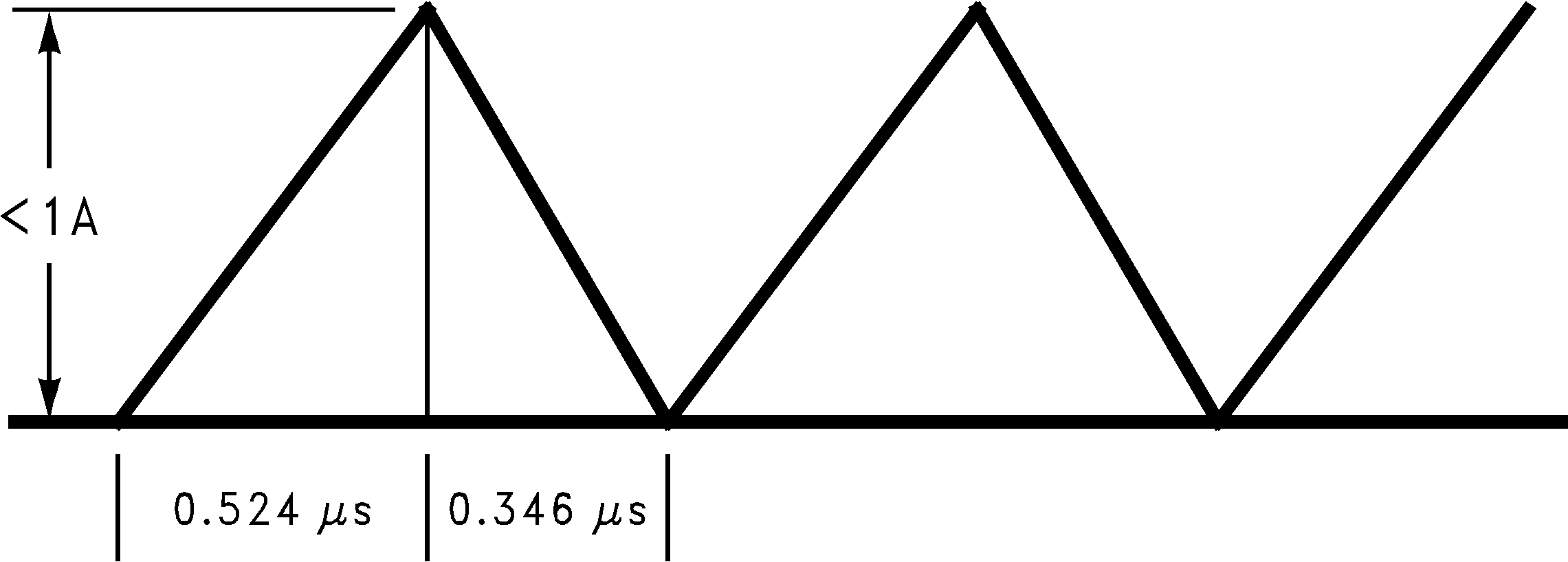
The minimum inductance should be selected such that the inductor (switch) current peak on each cycle does not reach the 1-A current limit maximum. To understand how to do this, an example will be presented.
In the example, the LM2733X will be used (nominal switching frequency 1.6 MHz, minimum switching frequency 1.15 MHz). This means the maximum cycle period is the reciprocal of the minimum frequency:
We will assume the input voltage is 5 V, VOUT = 12 V, VSW = 0.2 V, VDIODE = 0.3 V. The duty cycle is:
Duty Cycle = 60.3%
Therefore, the maximum switch ON time is 0.524 µs. An inductor should be selected with enough inductance to prevent the switch current from reaching 1A in the 0.524 µs ON time interval (see below):
 Figure 30. Discontinuous Design, 5V–12V Boost (LM2733X)
 The voltage across the inductor during ON time is 4.8V. Minimum inductance value is found by:
In this case, a 2.7 µH inductor could be used assuming it provided at least that much inductance up to the 1A current value. This same analysis can be used to find the minimum inductance for any boost application. Using the slower switching “Y” version requires a higher amount of minimum inductance because of the longer switching period.