SNVS100F March 2000 – July 2014 LM2937
PRODUCTION DATA.
- 1 Features
- 2 Applications
- 3 Description
- 4 Revision History
- 5 Pin Configuration and Functions
-
6 Specifications
- 6.1 Absolute Maximum Ratings
- 6.2 Handling Ratings
- 6.3 Recommended Operating Conditions
- 6.4 Thermal Information
- 6.5 Electrical Characteristics: LM2937-5
- 6.6 Electrical Characteristics: LM2937-8
- 6.7 Electrical Characteristics: LM2937-10
- 6.8 Electrical Characteristics: LM2937-12
- 6.9 Electrical Characteristics: LM2937-15
- 6.10 Typical Characteristics
- 7 Detailed Description
- 8 Application and Implementation
- 9 Power Supply Recommendations
- 10Layout
- 11Device and Documentation Support
- 12Mechanical, Packaging, and Orderable Information
7 Detailed Description
7.1 Overview
The LM2937 is a positive voltage regulator capable of supplying up to 500 mA of load current. The use of a PNP power transistor provides a low dropout voltage characteristic. With a load current of 500 mA the minimum input to output voltage differential required for the output to remain in regulation is typically 0.5 V (1 V ensured maximum over the full operating temperature range). Special circuitry has been incorporated to minimize the quiescent current to typically only 10 mA with a full 500-mA load current when the input to output voltage differential is greater than 3 V.
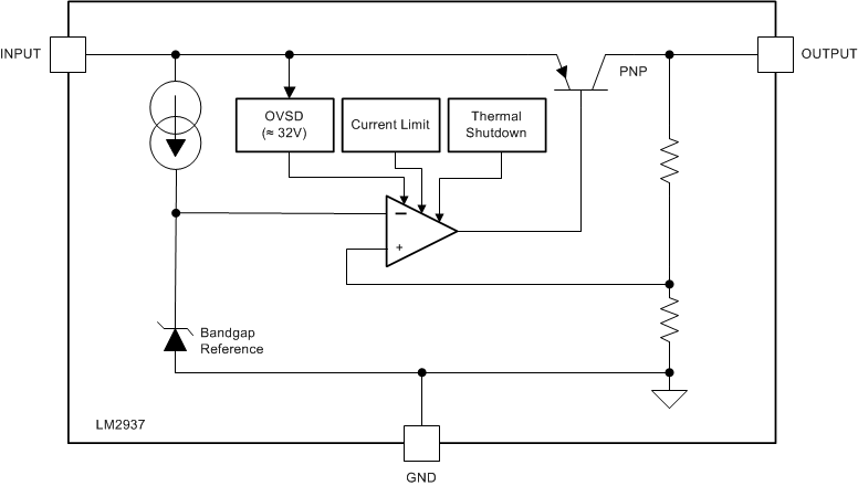
7.2 Functional Block Diagram
7.3 Feature Description
7.3.1 Thermal Shutdown (TSD)
The Thermal Shutdown circuitry of the LM2937 has been designed to protect the device against temporary thermal overload conditions. The TSD circuitry is not intended to replace proper heat-sinking. Continuously running the LM2937 device at thermal shutdown may degrade device reliability as the junction temperature will be exceeding the absolute maximum junction temperature rating.
7.3.2 Short Circuit Current Limit
The output current limiting circuitry of the LM2937 has been designed to limit the output current in cases where the load impedance is unusually low. This includes situations where the output may be shorted directly to ground. Continuous operation of the LM2937 at the current limit will typically result in the LM2937 transitioning into Thermal Shutdown mode.
7.3.3 Overvoltage Shutdown (OVSD)
Input voltages greater than typically 32 V will cause the LM2937 output to be disabled. When operating with the input voltage greater than the maximum recommended input voltage of 26 V the device performance is not ensured. Continuous operation with the input voltage greater than the maximum recommended input voltage is discouraged.
7.4 Device Functional Modes
The LM2937 design does not include any undervoltage lock-out (UVLO), or enable functions. Generally, the output voltage will track the input voltage until the input voltage is greater than VOUT + 1V. When the input voltage is greater than VOUT + 1V the LM2937 will be in linear operation, and the output voltage will be regulated; however, the device will be sensitive to any small perturbation of the input voltage. Device dynamic performance is improved when the input voltage is at least 2 V greater than the output voltage.