SNVS239C October 2004 – October 2015 LM3475
PRODUCTION DATA.
- 1 Features
- 2 Applications
- 3 Description
- 4 Revision History
- 5 Pin Configuration and Functions
- 6 Specifications
- 7 Detailed Description
-
8 Application and Implementation
- 8.1 Application Information
- 8.2
Typical Application
- 8.2.1 Design Requirements
- 8.2.2
Detailed Design Procedure
- 8.2.2.1 Setting Output Voltage
- 8.2.2.2 Setting Operating Frequency and Output Ripple
- 8.2.2.3 Using a Feed-forward Capacitor
- 8.2.2.4 Inductor Selection
- 8.2.2.5 Output Capacitor Selection
- 8.2.2.6 Input Capacitor Selection
- 8.2.2.7 Diode Selection
- 8.2.2.8 P-Channel MOSFET Selection
- 8.2.2.9 Reducing Switching Noise
- 8.2.3 Application Curves
- 9 Power Supply Recommendations
- 10Layout
- 11Device and Documentation Support
- 12Mechanical, Packaging, and Orderable Information
6 Specifications
6.1 Absolute Maximum Ratings
See (2)(1)| MIN | MAX | UNIT | |||
|---|---|---|---|---|---|
| VIN | −0.3 | 16 | V | ||
| PGATE | −0.3 | 16 | V | ||
| FB | −0.3 | 5 | V | ||
| EN | −0.3 | 16 | V | ||
| Power dissipation (3) | 440 | mW | |||
| Lead temperature | Vapor phase (60 s) | 215 | °C | ||
| Infrared (15 s) | 220 | ||||
| Tstg | Storage temperature | −65 | 1150 | °C | |
(1) If Military/Aerospace specified devices are required, please contact the Texas Instruments Sales Office/ Distributors for availability and specifications.
(2) Stresses beyond those listed under Absolute Maximum Ratings may cause permanent damage to the device. These are stress ratings only, which do not imply functional operation of the device at these or any other conditions beyond those indicated under Recommended Operating Conditions. Exposure to absolute-maximum-rated conditions for extended periods may affect device reliability.
(3) The maximum allowable power dissipation is a function of the maximum junction temperature, TJ_MAX, the junction-to-ambient thermal resistance, θJA and the ambient temperature, TA. The maximum allowable power dissipation at any ambient temperature is calculated using: PD_MAX = (TJ_MAX - TA)/θJA. The maximum power dissipation of 0.44 W is determined using TA = 25°C, θJA = 225°C/W, and TJ_MAX = 125°C.
6.2 ESD Ratings
over operating free-air temperature range (unless otherwise noted)| VALUE | UNIT | |||
|---|---|---|---|---|
| V(ESD) | Electrostatic discharge | Human-body model (HBM), per ANSI/ESDA/JEDEC JS-001(1) | 2500 | V |
(1) JEDEC document JEP155 states that 500-V HBM allows safe manufacturing with a standard ESD control process.
6.3 Recommended Operating Ratings
| MIN | NOM | MAX | UNIT | ||
|---|---|---|---|---|---|
| Supply voltage | 2.7 | 10 | V | ||
| TJ | Operating junction temperature | -40 | 125 | °C | |
6.4 Thermal Information
| THERMAL METRIC(1) | LM3475 | UNIT | |
|---|---|---|---|
| DBV (SOT-23) | |||
| 5 PINS | |||
| RθJA | Junction-to-ambient thermal resistance | 164.2 | °C/W |
| RθJC(top) | Junction-to-case (top) thermal resistance | 115.3 | °C/W |
| RθJB | Junction-to-board thermal resistance | 27.0 | °C/W |
| ψJT | Junction-to-top characterization parameter | 12.8 | °C/W |
| ψJB | Junction-to-board characterization parameter | 26.5 | °C/W |
| RθJC(bot) | Junction-to-case (bottom) thermal resistance | N/A | °C/W |
(1) For more information about traditional and new thermal metrics, see the Semiconductor and IC Package Thermal Metrics application report, SPRA953.
6.5 Electrical Characteristics
Typical limits are for TJ = 25°C, unless otherwise specified, VIN = EN = 5.0 V. Maximum and minimum specification limits are specified by design, test, or statistical analysis.| PARAMETER | TEST CONDITIONS | MIN | TYP | MAX | UNIT | ||
|---|---|---|---|---|---|---|---|
| IQ | Quiescent current | EN = VIN (PGATE Open) | TJ = 25°C | 260 | µA | ||
| TJ = −40°C to +125°C | 170 | 320 | |||||
| EN = 0V | TJ = 25°C | 7 | |||||
| TJ = −40°C to +125°C | 4 | 10 | |||||
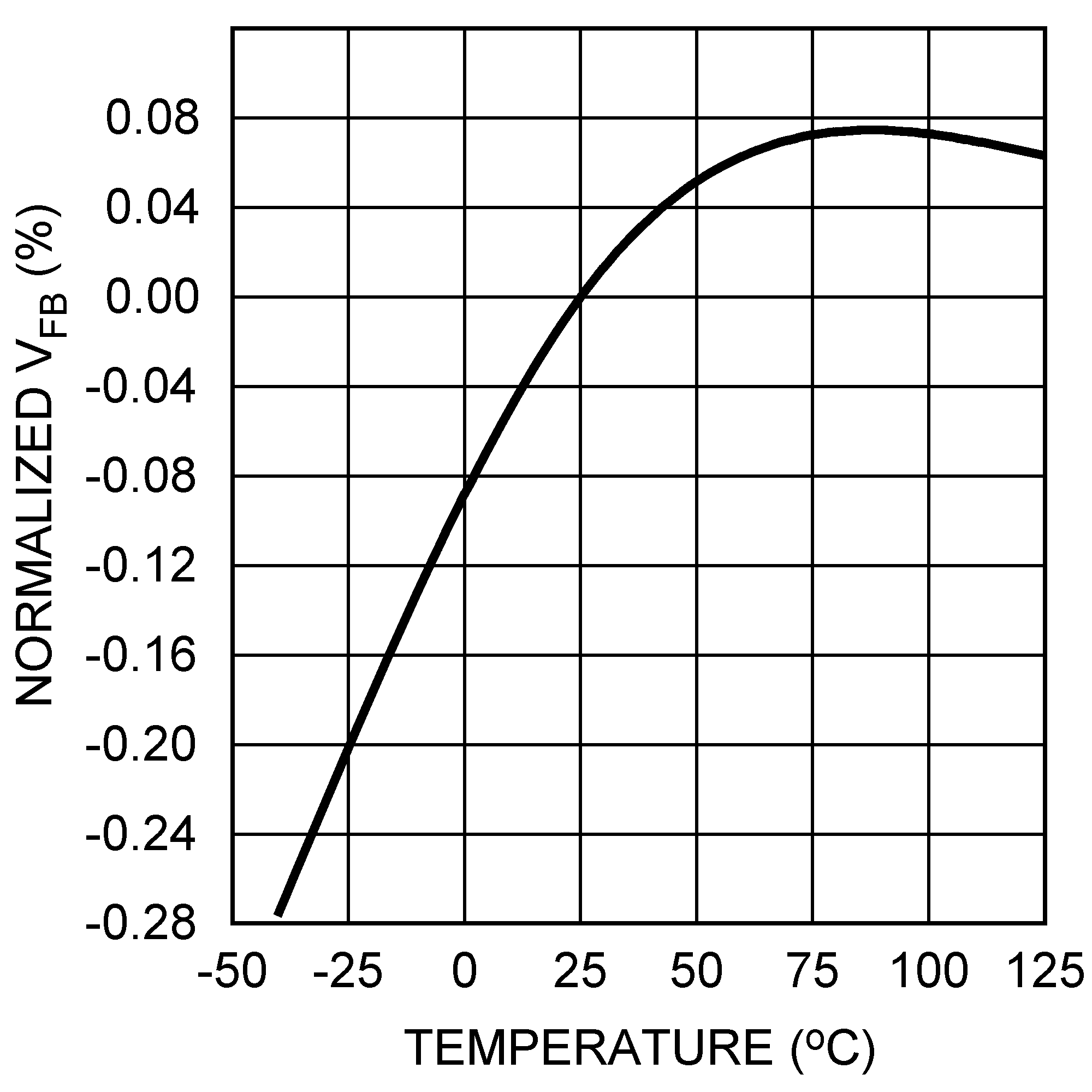
| VFB | Feedback voltage | TJ = 25°C | 0.8 | V | |||
| TJ = −40°C to +125°C | 0.788 | 0.812 | |||||
| %ΔVFB/ΔVIN | Feedback voltage line regulation | 2.7 V < VIN < 10 V | 0.01 | %/V | |||
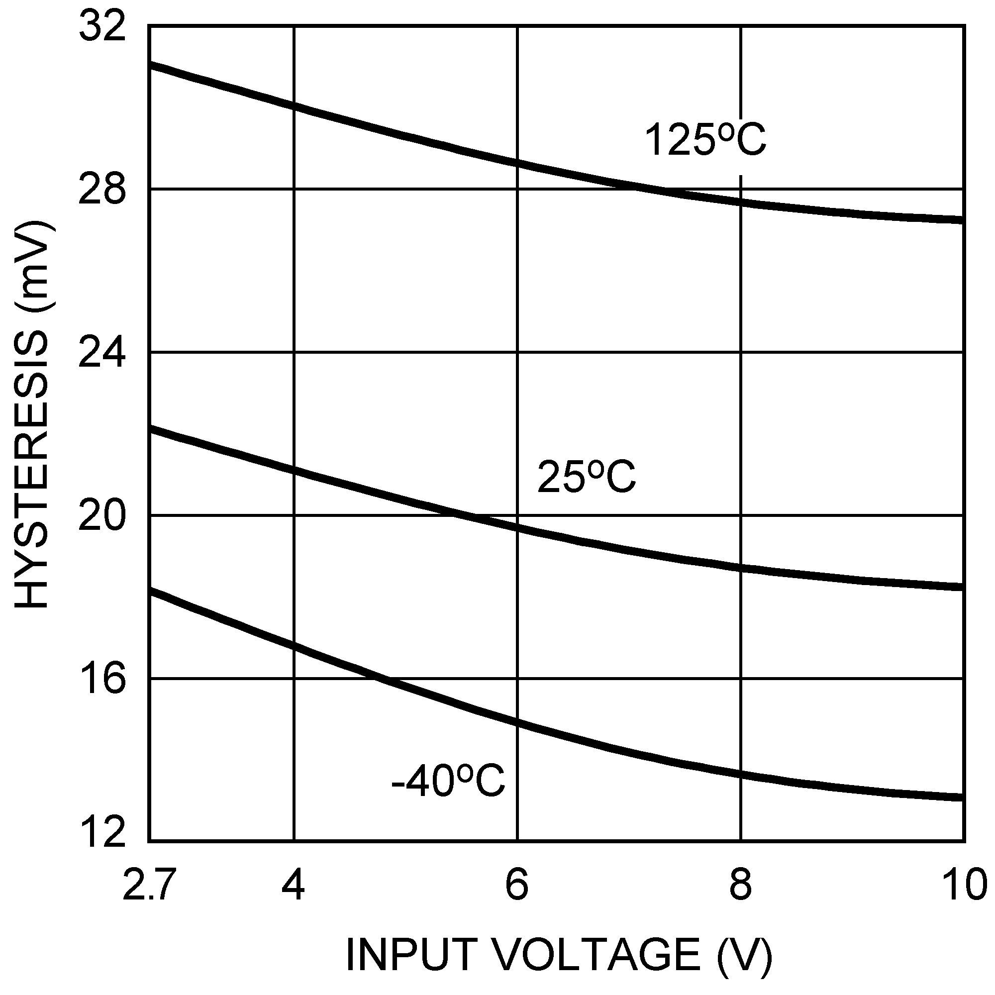
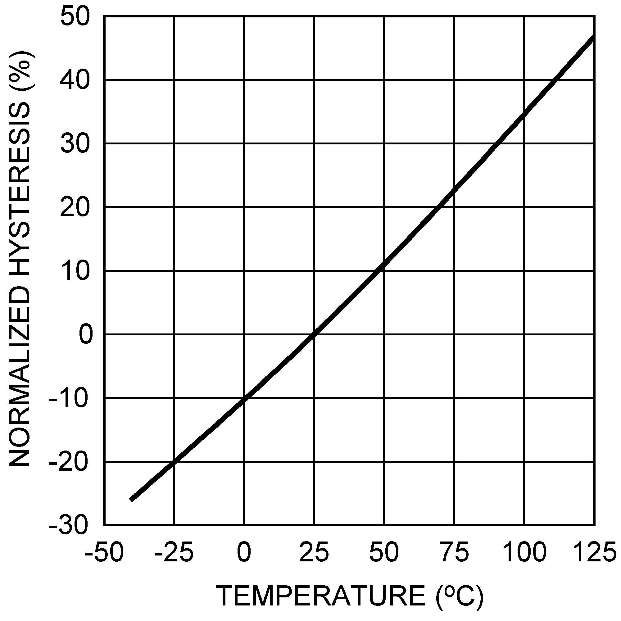
| VHYST | Comparator hysteresis | 2.7 V < VIN < 10 V | TJ = 25°C | 21 | 28 | mV | |
| −40°C to +125°C | 21 | 32 | |||||
| IFB | FB bias current | TJ = 25°C | 50 | nA | |||
| −40°C to +125°C | 600 | ||||||
| VthEN | Enable threshold voltage | Increasing | TJ = 25°C | 1.5 | V | ||
| −40°C to +125°C | 1.2 | 1.8 | |||||
| Hysteresis | 365 | mV | |||||
| IEN | Enable leakage current | EN = 10 V | TJ = 25°C | 0.025 | µA | ||
| −40°C to +125°C | 1 | ||||||
| RPGATE | Driver resistance | Source ISOURCE = 100 mA |
2.8 | Ω | |||
| Sink ISink = 100 mA |
1.8 | ||||||
| IPGATE | Driver output current | Source VPGATE = 3.5 V CPGATE = 1 nF |
0.475 | A | |||
| Sink VPGATE = 3.5 V CPGATE = 1 nF |
1.0 | ||||||
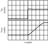
| TSS | Soft-start time | 2.7 V < VIN < 10 V (EN Rising) | 4 | ms | |||
| TONMIN | Minimum on-time | PGATE Open | 180 | ns | |||
| VUVD | Undervoltage detection | Measured at the FB Pin | TJ = 25°C | 0.56 | V | ||
| −40°C to +125°C | 0.487 | 0.613 | |||||
6.6 Typical Characteristics
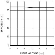
Unless specified otherwise, all curves taken at VIN = 5 V, VOUT = 2.5 V, L = 10 µH, COUT = 100 µF, ESR = 100 mΩ, and TA = 25°C.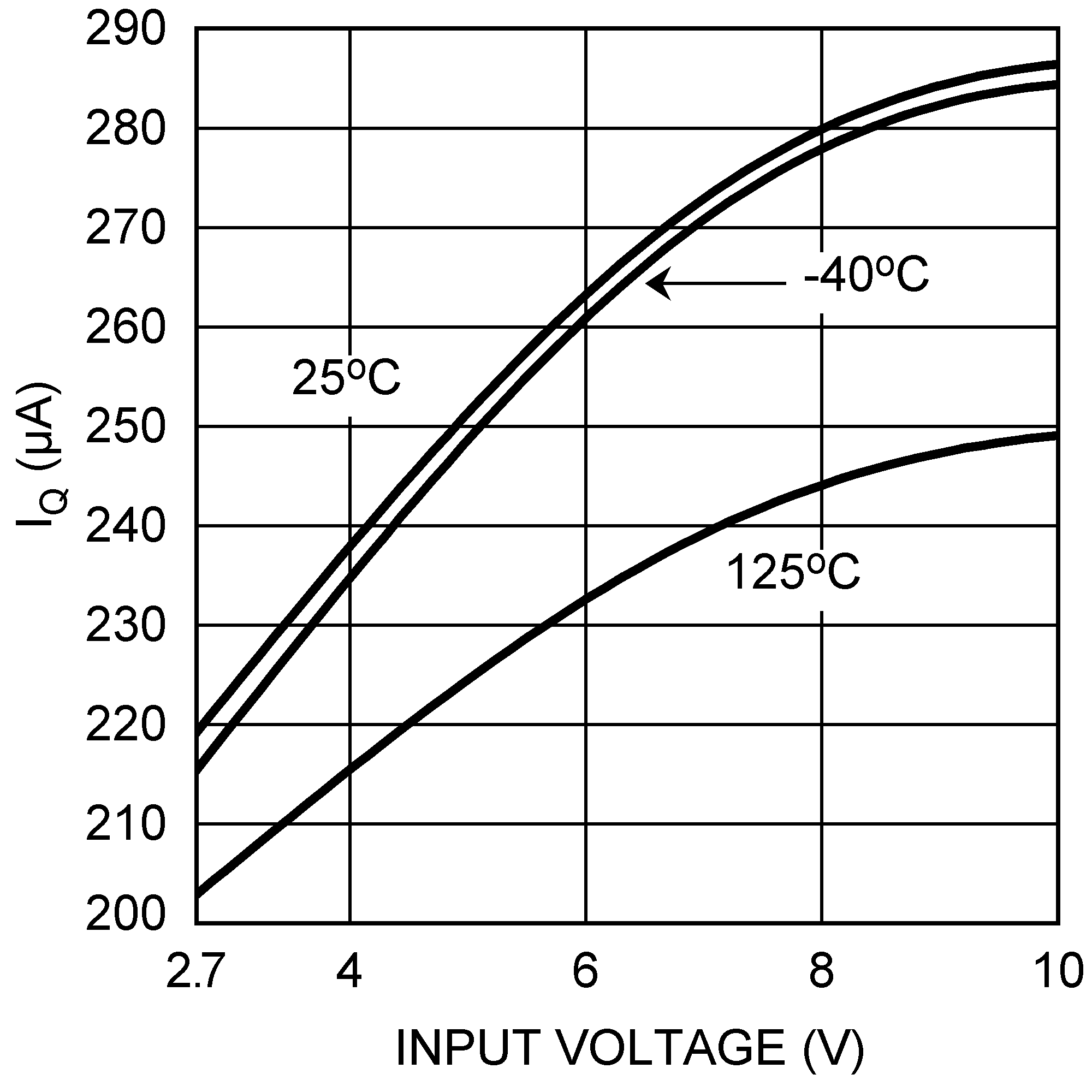
| IOUT = 2 A |
