JAJS711X July 2000 – June 2017 LM3478
PRODUCTION DATA.
- 1 特長
- 2 アプリケーション
- 3 説明
- 4 改訂履歴
- 5 Pin Configuration and Functions
- 6 Specifications
- 7 Detailed Description
-
8 Application and Implementation
- 8.1 Application Information
- 8.2
Typical Applications
- 8.2.1
Typical High Efficiency Step-Up (Boost) Converter
- 8.2.1.1 Design Requirements
- 8.2.1.2
Detailed Design Procedure
- 8.2.1.2.1 Custom Design with WEBENCH Tools
- 8.2.1.2.2 Power Inductor Selection
- 8.2.1.2.3 Programming the Output Voltage
- 8.2.1.2.4 Setting the Current Limit
- 8.2.1.2.5 Current Limit with External Slope Compensation
- 8.2.1.2.6 Power Diode Selection
- 8.2.1.2.7 Power MOSFET Selection
- 8.2.1.2.8 Input Capacitor Selection
- 8.2.1.2.9 Output Capacitor Selection
- 8.2.1.2.10 Compensation
- 8.2.1.3 Application Curves
- 8.2.2 Typical SEPIC Converter
- 8.2.1
Typical High Efficiency Step-Up (Boost) Converter
- 9 Power Supply Recommendations
- 10Layout
- 11デバイスおよびドキュメントのサポート
- 12メカニカル、パッケージ、および注文情報
パッケージ・オプション
メカニカル・データ(パッケージ|ピン)
サーマルパッド・メカニカル・データ
発注情報
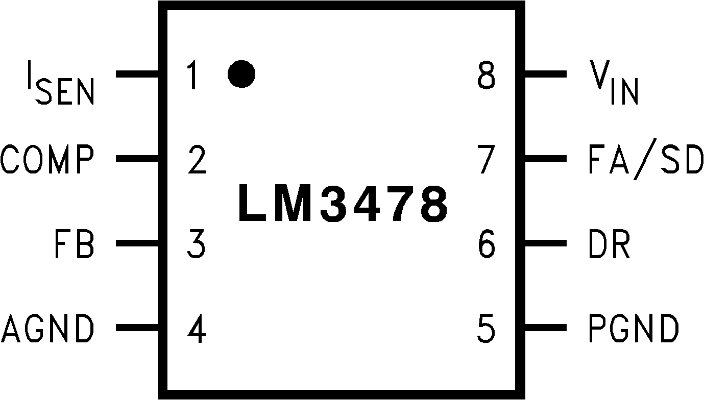
5 Pin Configuration and Functions
8-Lead VSSOP-8 Package
3 Pins
Top View

8-Lead SOIC-8
3 Pins
Top View

Pin Functions
| PIN | I/O | DESCRIPTION | |
|---|---|---|---|
| NAME | NO. | ||
| ISEN | 1 | I | Current sense input pin. Voltage generated across an external sense resistor is fed into this pin. |
| COMP | 2 | I | Compensation pin. A resistor, capacitor combination connected to this pin provides compensation for the control loop. |
| FB | 3 | I | Feedback pin. The output voltage should be adjusted using a resistor divider to provide 1.26 V at this pin. |
| AGND | 4 | G | Analog ground pin. |
| PGND | 5 | G | Power ground pin. |
| DR | 6 | O | Drive pin. The gate of the external MOSFET should be connected to this pin. |
| FA/SD | 7 | I | Frequency adjust and Shutdown pin. A resistor connected to this pin sets the oscillator frequency. A high level on this pin for longer than 30 µs will turn the device off. The device will then draw less than 10µA from the supply. |
| VIN | 8 | P | Power Supply Input pin. |