8 Specifications
8.1 Absolute Maximum Ratings
over operating free-air temperature range (unless otherwise noted)(1)(2)
|
MIN |
MAX |
UNIT |
| IN, SW, OUT, LED1, LED2 |
−0.3 |
6 |
V |
| SDA, SCL, TX, TORCH/TEMP, HWEN, STROBE |
−0.3 to the lesser of (VIN+0.3) w/ 6 V max |
| Continuous power dissipation(3) |
Internally limited |
|
| Junction temperature (TJ-MAX) |
|
150 |
°C |
| Maximum lead temperature (soldering) |
Note (4) |
|
(1) Stresses beyond those listed under Absolute Maximum Ratings may cause permanent damage to the device. These are stress ratings only, which do not imply functional operation of the device at these or any other conditions beyond those indicated under Recommended Operating Conditions. Exposure to absolute-maximum-rated conditions for extended periods may affect device reliability.
(2) All voltages are with respect to the potential at the GND terminal.
(3) Internal thermal shutdown circuitry protects the device from permanent damage. Thermal shutdown engages at TJ = 150°C (typ.) and disengages at TJ = 135°C (typ.). Thermal shutdown is ensured by design.
(4) For detailed soldering specifications and information, please refer to TI Application Note
DSBGA Wafer Level Chip Scale Package (
SNVA009).
8.2 Handling Ratings
|
MIN |
MAX |
UNIT |
| Tstg |
Storage temperature range |
−65 |
150 |
°C |
| V(ESD) |
Electrostatic discharge |
Human body model (HBM), per ANSI/ESDA/JEDEC JS-001, all pins(1) |
−2500 |
2500 |
V |
| Charged device model (CDM), per JEDEC specification JESD22-C101, all pins(2) |
−1500 |
1500 |
(1) JEDEC document JEP155 states that 500-V HBM allows safe manufacturing with a standard ESD control process.
(2) JEDEC document JEP157 states that 250-V CDM allows safe manufacturing with a standard ESD control process.
8.3 Recommended Operating Conditions
over operating free-air temperature range (unless otherwise noted)(1)(2)
|
MIN |
MAX |
UNIT |
| VIN |
2.5 |
5.5 |
V |
| Junction temperature (TJ) |
|
−40 |
125 |
°C |
| Ambient temperature (TA) (3) |
|
−40 |
85 |
(1) Stresses beyond those listed under absolute maximum ratings may cause permanent damage to the device. These are stress ratings only, and functional operation of the device at these or any other conditions beyond those indicated under recommended operating conditions is not implied. Exposure to absolute-maximum-rated conditions for extended periods may affect device reliability.
(2) All voltages are with respect to the potential at the GND terminal.
(3) In applications where high power dissipation and/or poor package thermal resistance is present, the maximum ambient temperature may have to be derated. Maximum ambient temperature (TA-MAX) is dependent on the maximum operating junction temperature (TJ-MAX-OP = 125°C), the maximum power dissipation of the device in the application (PD-MAX), and the junction-to-ambient thermal resistance of the part/package in the application (RθJA), as given by the following equation: TA-MAX = TJ-MAX-OP – (RθJA × PD-MAX).
8.4 Thermal Information
| THERMAL METRIC(1) |
LM3643 |
UNIT |
| DSBGA |
| 12 PINS |
| RθJA |
Junction-to-ambient thermal resistance |
67.8 |
°C/W |
(1) For more information about traditional and new thermal metrics, see the
IC Package Thermal Metrics application report,
SPRA953.
8.5 Electrical Characteristics
Typical limits tested at TA = 25°C. Minimum and maximum limits apply over the full operating ambient temperature range (−40°C ≤ TA ≤ 85°C). Unless otherwise specified, VIN = 3.6 V, HWEN = VIN.(1)(2)
| PARAMETER |
TEST CONDITIONS |
MIN |
TYP |
MAX |
UNIT |
| CURRENT SOURCE SPECIFICATIONS |
| ILED1/2 |
Current source accuracy |
VOUT = 4 V, flash code = 0x7F = 1.5 A flash |
–7% |
1.5 |
7% |
A |
| VOUT = 4 V, torch code = 0x3F = 89.3 mA torch |
–10% |
89.3 |
10% |
mA |
| VHR |
LED1 and LED2 current source regulation voltage |
ILED1/2 = 729 mA |
Flash |
|
290 |
|
mV |
| ILED1/2 = 179 mA |
Torch |
|
158 |
|
| VOVP |
|
ON threshold |
4.86 |
5 |
5.1 |
V |
| OFF threshold |
4.75 |
4.88 |
4.99 |
| STEP-UP DC/DC CONVERTER SPECIFICATIONS |
| RPMOS |
PMOS switch on-resistance |
|
|
86 |
|
mΩ |
| RNMOS |
NMOS switch on-resistance |
|
|
65 |
|
| ICL |
Switch current limit |
Reg 0x07, bit[0] = 0 |
–12% |
1.9 |
12% |
A |
| Reg 0x07, bit[0] = 1 |
–12% |
2.8 |
12% |
| UVLO |
Undervoltage lockout threshold |
Falling VIN |
–2% |
2.5 |
2% |
V |
| VTRIP |
NTC comparator trip threshold |
Reg 0x09, bits[3:1] = '100' |
–5% |
0.6 |
5% |
V |
| INTC |
NTC current |
|
–6% |
50 |
6% |
µA |
| VIVFM |
Input voltage flash monitor trip threshold |
Reg 0x02, bits[5:3] = '000' |
–3% |
2.9 |
3% |
V |
| IQ |
Quiescent supply current |
Device not switching pass mode |
|
0.3 |
0.75 |
mA |
| ISD |
Shutdown supply current |
Device disabled, HWEN = 0 V
2.5 V ≤ VIN ≤ 5.5 V |
|
0.1 |
4 |
µA |
| ISB |
Standby supply current |
Device disabled, HWEN = 1.8 V
2.5 V ≤ VIN ≤ 5.5 V |
|
2.5 |
10 |
µA |
| HWEN, TORCH/TEMP, STROBE, TX VOLTAGE SPECIFICATIONS |
| VIL |
Input logic low |
2.5 V ≤ VIN ≤ 5.5 V |
0 |
|
0.4 |
V |
| VIH |
Input logic high |
1.2 |
|
VIN |
| I2C-COMPATIBLE INTERFACE SPECIFICATIONS (SCL, SDA) |
| VIL |
Input logic low |
2.5 V ≤ VIN ≤ 4.2 V |
0 |
|
0.4 |
V |
| VIH |
Input logic high |
1.2 |
|
VIN |
| VOL |
Output logic low |
ILOAD = 3 mA |
|
|
400 |
mV |
(1) Minimum (Min) and Maximum (Max) limits are specified by design, test, or statistical analysis. Typical (typ.) numbers are not verified, but do represent the most likely norm. Unless otherwise specified, conditions for typical specifications are: VIN = 3.6 V and TA = 25°C.
(2) All voltages are with respect to the potential at the GND pin.
8.6 Timing Requirements
|
MIN |
NOM |
MAX |
UNIT |
| t1 |
SCL clock period |
2.4 |
|
|
µs |
| t2 |
Data in set-up time to SCL high |
100 |
|
|
ns |
| t3 |
Data out stable After SCL low |
0 |
|
|
| t4 |
SDA low set-up time to SCL Low (start) |
100 |
|
|
| t5 |
SDA high hold time after SCL high (stop) |
100 |
|
|
8.7 Switching Characteristics
over operating free-air temperature range (unless otherwise noted)
| PARAMETER |
TEST CONDITIONS |
MIN |
TYP |
MAX |
UNIT |
| ƒSW |
Switching frequency |
2.5 V ≤ VIN ≤ 5.5 V |
–6% |
4 |
6% |
MHz |
8.8 Typical Characteristics
Ambient temperature is 25°C, input voltage is 3.6 V, HWEN = VIN, CIN = COUT = 2 × 10 µF and L = 1 µH, unless otherwise noted .
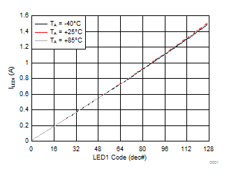 Figure 2. LED1 Flash Current vs Brightness Code
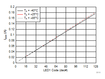 Figure 4. LED1 Torch Current vs Brightness Code
 Figure 6. LED1 Current vs Input Voltage
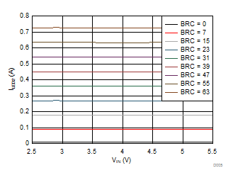 Figure 8. LED2 Current vs Input Voltage
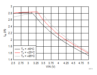
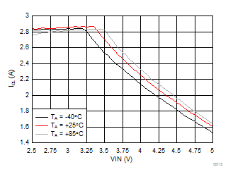
| ILED = 1.5 A |
ƒSW = 2 MHz |
Flash |
|
|
|
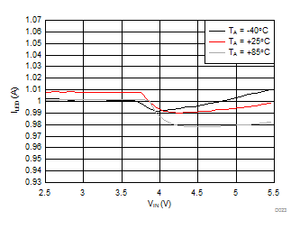
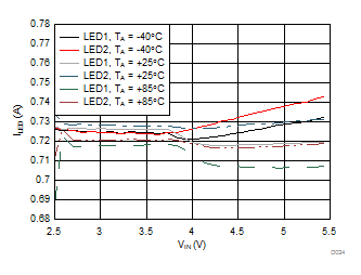
Figure 10. LED1/2 Current vs Input Voltage
| ILED = 1 A |
ƒSW = 2 MHz |
Flash |
|
|
|
Figure 12. LED1/2 Current vs Input Voltage
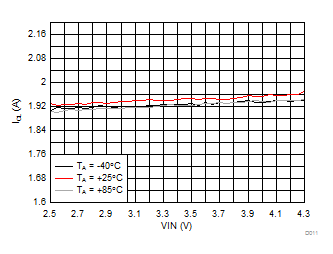
| ILED = 179 mA |
ƒSW = 2 MHz |
Torch |
|
|
|
Figure 14. LED Current vs Input Voltage
| ILED = 179 mA |
ƒSW = 2 MHz |
Torch |
|
|
|
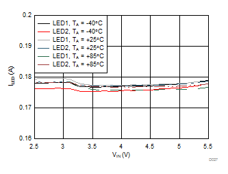
Figure 16. LED1 and LED2 Current vs Input Voltage
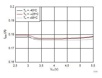
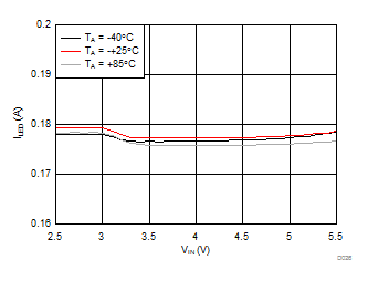
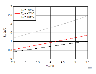 Figure 18. Standby Current vs Input Voltage
 Figure 20. Standby Current vs Input Voltage
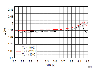
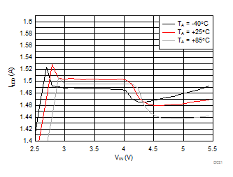
| ILED = 1.5 A |
ƒSW = 4 MHz |
VLED = 4.5 V |
| ICL = 1.9 A |
|
|
Figure 22. Inductor Current Limit vs Input Voltage
| ILED = 1.5 A |
ƒSW = 4 MHz |
VLED = 4.5 V |
| ICL = 2.8 A |
|
|
Figure 24. Inductor Current Limit vs Input Voltage
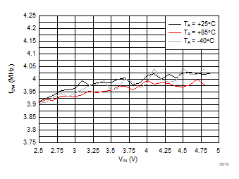 Figure 26. 4-MHz Switching Frequency vs Input Voltage
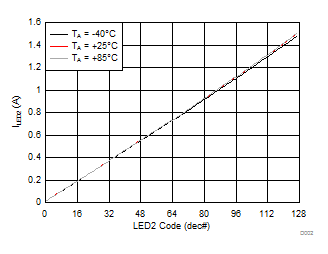 Figure 3. LED2 Flash Current vs Brightness Code
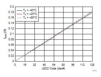 Figure 5. LED2 Torch Current vs Brightness Code
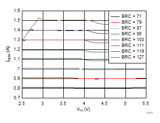 Figure 7. LED1 Current vs Input Voltage
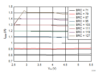 Figure 9. LED2 Current vs Input Voltage
| ILED = 1.5 A |
ƒSW = 4 MHz |
Flash |
|
|
|
Figure 11. LED1/2 Current vs Input Voltage
| ILED = 730 mA |
ƒSW = 2 MHz |
Flash |
|
|
|
Figure 13. LED1 and LED2 Current vs Input Voltage
| ILED = 179 mA |
ƒSW = 4 MHz |
Torch |
|
|
|
Figure 15. LED Current vs Input Voltage
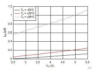 Figure 17. Shutdown Current vs Input Voltage
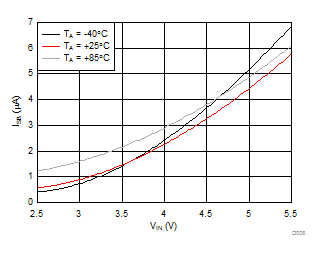 Figure 19. Standby Current vs Input Voltage
| ILED = 1.5 A |
ƒSW = 2 MHz |
VLED = 4.5 V |
| ICL = 1.9 A |
|
|
Figure 21. Inductor Current Limit vs Input Voltage
| ILED = 1.5 A |
ƒSW = 2 MHz |
VLED = 4.5 V |
| ICL = 2.8 A |
|
|
Figure 23. Inductor Current Limit vs Input Voltage
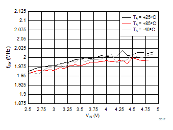 Figure 25. 2-MHz Switching Frequency vs Input Voltage
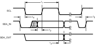 Figure 1. I2C-Compatible Interface Specifications