SNAS513F August 2011 – November 2015 LM48560
PRODUCTION DATA.
- 1 Features
- 2 Applications
- 3 Description
- 4 Revision History
- 5 Pin Configuration and Functions
- 6 Specifications
- 7 Parameter Measurement Information
- 8 Detailed Description
- 9 Application and Implementation
- 10Power Supply Recommendations
- 11Layout
- 12Device and Documentation Support
- 13Mechanical, Packaging, and Orderable Information
9 Application and Implementation
NOTE
Information in the following applications sections is not part of the TI component specification, and TI does not warrant its accuracy or completeness. TI’s customers are responsible for determining suitability of components for their purposes. Customers should validate and test their design implementation to confirm system functionality.
9.1 Application Information
The LM48560 device is a high voltage, high efficiency Class H driver for ceramic speakers and piezo actuators. The integrated, high efficiency boost converter dynamically adjusts the amplifier’s supply voltage based on the output signal to increase headroom and improve efficiency. The LM48560 device’s Class H architecture offers significant power savings compared to traditional Class AB amplifiers. The device provides 30Vp-p output drive while consuming just 4 mA of quiescent current from a 3.6 V supply.
The LM48560 device features two fully differential inputs with separate gain settings, and a selectable control interface. In software control mode, the gain control and device modes are configured through the I2C interface. In hardware control mode, the gain and input mux are configured through a pair of logic inputs. The LM48560 device has a low current shutdown mode that disables the amplifier and boost converter and reduces quiescent current consumption to 0.1 μA.
9.2 Typical Application
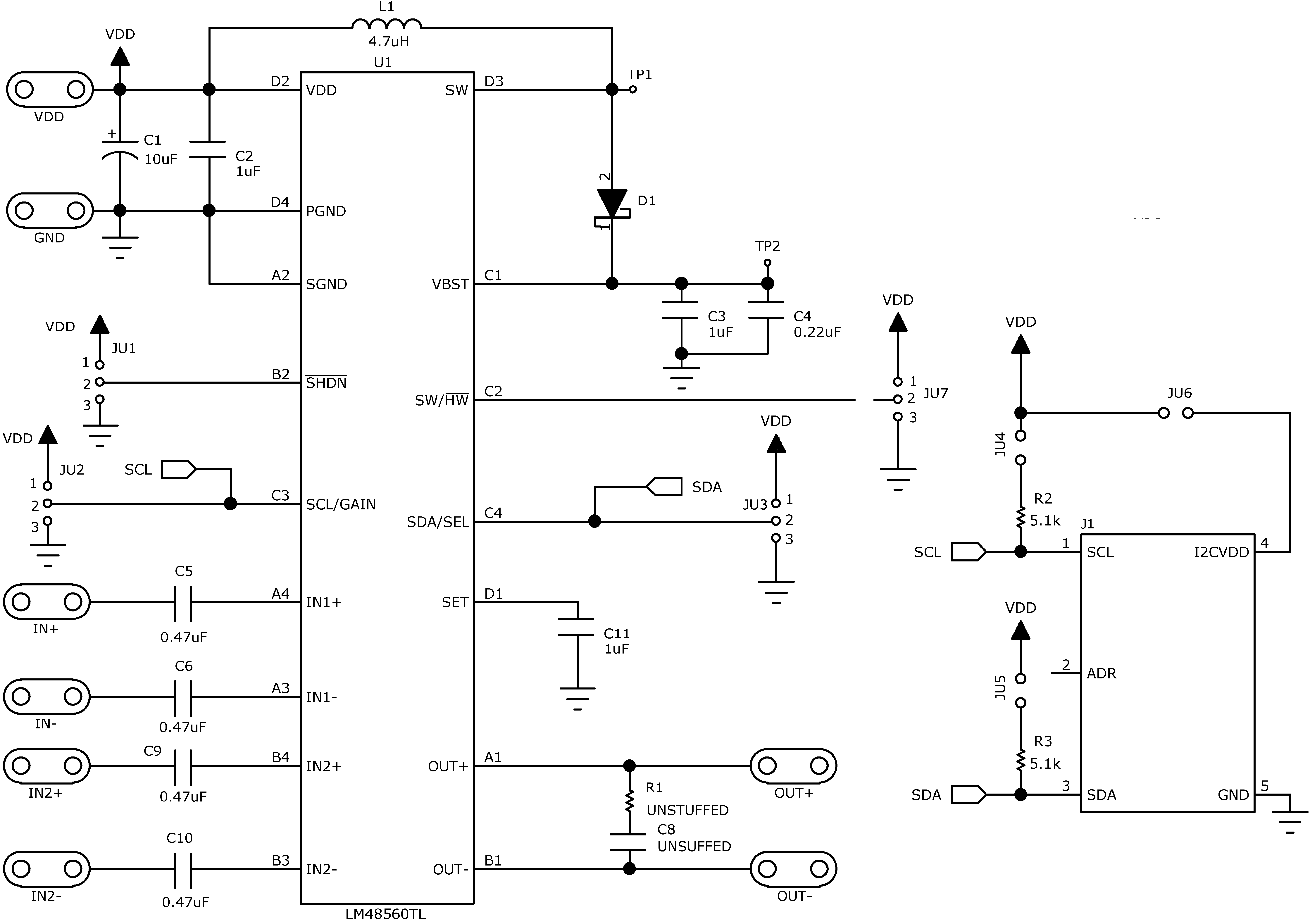
 Figure 28. Demo Board Schematic
9.2.1 Design Requirements
Table 10 shows the design parameters for this design example.
Table 10. Design Parameters
| PARAMETERS | VALUES |
|---|---|
| Supply voltage | 2.7 V to 5.5 V |
| Temperature | –40 °C to 85 °C |
| Input voltage | –0.3 V to Vdd 0.3 V |
9.2.2 Detailed Design Procedure
9.2.2.1 Proper Selection of External Components
9.2.2.1.1 ALC Timing (CSET) Capacitor Selection
The recommended range value of CSET is between 0.01 μF to 1 μF. Lowering the value below 0.01 μF can increase the attack time but LM48560 device ALC ability to regulate its output can be disrupted and approaches the hard limiter circuit. This in turn increases the THD+N and audio quality will be severely affected.
9.2.2.1.2 Power Selection of External Components
Proper power supply bypassing is critical for low noise performance and high PSRR. Place the supply bypass capacitors as close to the device as possible. Place a 1-µF ceramic capacitor from VDD to GND. Additional bulk capacitance may be added as required.
9.2.2.1.3 Boost Converter Capacitor Selection
The LM48560 device boost converter requires three external capacitors for proper operation: a 1-μF supply bypass capacitor, and 1-μF + 100-pF output reservoir capacitors. Place the supply bypass capacitor as close to VDD as possible. Place the reservoir capacitors as close to VBST and VAMP as possible. Low ESR surface-mount multi-layer ceramic capacitors with X7R or X5R temperature characteristics are recommended. Select output capacitors with voltage rating of 25 V or higher. Tantalum, OS-CON and aluminum electrolytic capacitors are not recommended.
9.2.2.1.4 Inductor Selection
The LM48560 device boost converter is designed for use with a 4.7-μH inductor. Choose an inductor with a saturation current rating greater than the maximum operating peak current of the LM48560 device (> 1A). This ensures that the inductor does not saturate, preventing excess efficiency loss, over heating and possible damage to the inductor. Additionally, choose an inductor with the lowest possible DCR (series resistance) to further minimize efficiency losses.
9.2.2.1.5 Diode Selection
Use a Schottkey diode as shown in Figure 28. A 20-V diode such as the NSR0520V2T1G from On Semiconductor is recommended. The NSR0520V2T1G is designed to handle a maximum average current of 500 mA.
9.2.3 Application Curve
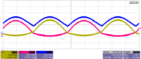
 Figure 29. Out+, Out– and Vbst Waveforms for a 100 Hz Input Sine Wave