SNVS359E May 2005 – December 2014 LM5021
PRODUCTION DATA.
- 1 Features
- 2 Applications
- 3 Description
- 4 Revision History
- 5 Pin Configuration and Functions
- 6 Specifications
- 7 Detailed Description
- 8 Application and Implementation
- 9 Power Supply Recommendations
- 10Layout
- 11Device and Documentation Support
- 12Mechanical, Packaging, and Orderable Information
5 Pin Configuration and Functions
8-Pin VSSOPand PDIP
Packages DGK and P
(Top View)
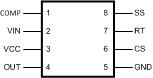
Pin Functions
| PIN | I/O | DESCRIPTION | APPLICATION INFORMATION | |
|---|---|---|---|---|
| NO. | NAME | |||
| 1 | COMP | I | Control input for the Pulse Width Modulator and Hiccup comparators. | COMP pull-up is provided by an internal 5K resistor which may be used to bias an opto-coupler transistor. |
| 2 | VIN | I | Input voltage. | Input to start-up regulator. The VIN pin is clamped at 36 V by an internal zener diode. |
| 3 | VCC | O | Output only of a linear bias supply regulator. Nominally 8.5 V. | VCC provides bias to controller and gate drive sections of the LM5021. An external capacitor must be connected from this pin to ground. |
| 4 | OUT | O | MOSFET gate driver output. | High current output to the external MOSFET gate input with source/sink current capability of 0.3 A and 0.7 A respectively. |
| 5 | GND | — | Ground return. | |
| 6 | CS | I | Current Sense input. | Current sense input for current mode control and over-current protection. Current limiting is accomplished using a dedicated current sense comparator. If the CS comparator input exceeds 0.5 V the OUT pin switches low for cycle-by-cycle current limit. CS is held low for 90ns after OUT switches high to blank the leading edge current spike. |
| 7 | RT / SYNC | O | Oscillator timing resistor pin and synchronization input. | An external resistor connected from RT to GND sets the oscillator frequency. This pin will also accept synchronization pulses from an external clock. |
| 8 | SS | O | Soft-start / Hiccup time | An external capacitor and an internal 22 µA current source set the soft-start ramp. The soft -start capacitor controls both the soft-start rate and the hiccup mode period. |