JAJSCV6B December 2016 – June 2017 LM5166
PRODUCTION DATA.
- 1 特長
- 2 アプリケーション
- 3 概要
- 4 改訂履歴
- 5 Pin Configuration and Functions
- 6 Specifications
-
7 Detailed Description
- 7.1 Overview
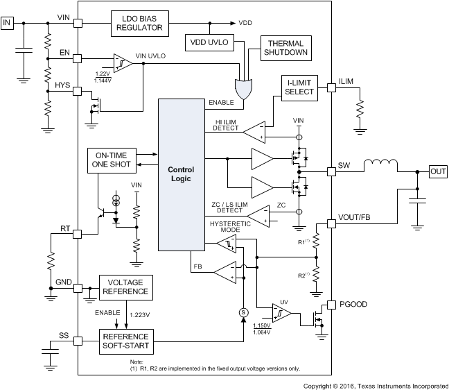
- 7.2 Functional Block Diagram
- 7.3
Feature Description
- 7.3.1 Integrated Power MOSFETs
- 7.3.2 Selectable PFM or COT Mode Converter Operation
- 7.3.3 Low Dropout Operation and 100% Duty Cycle Mode
- 7.3.4 Adjustable Output Voltage (FB)
- 7.3.5 Adjustable Current Limit
- 7.3.6 Precision Enable (EN) and Hysteresis (HYS)
- 7.3.7 Power Good (PGOOD)
- 7.3.8 Configurable Soft Start (SS)
- 7.3.9 Short-Circuit Operation
- 7.3.10 Thermal Shutdown
- 7.4 Device Functional Modes
-
8 Applications and Implementation
- 8.1 Application Information
- 8.2
Typical Applications
- 8.2.1
Design 1: Wide VIN, Low IQ, High-Efficiency COT Converter Rated at 5 V, 500 mA
- 8.2.1.1 Design Requirements
- 8.2.1.2
Detailed Design Procedure
- 8.2.1.2.1 Custom Design With WEBENCH® Tools
- 8.2.1.2.2 Feedback Resistors - RFB1, RFB2
- 8.2.1.2.3 Switching Frequency - RT
- 8.2.1.2.4 Filter Inductance - LF
- 8.2.1.2.5 Output Capacitors - COUT
- 8.2.1.2.6 Ripple Generation Network - RESR, CFF
- 8.2.1.2.7 Input Capacitor - CIN
- 8.2.1.2.8 Soft-Start Capacitor - CSS
- 8.2.1.2.9 Application Curves
- 8.2.2 Design 2: Wide VIN, Low IQ COT Converter Rated at 3.3 V, 500 mA
- 8.2.3 Design 3: High-Density PFM Converter Rated at 3.3 V, 0.3 A
- 8.2.4 Design 4: Wide VIN, Low IQ PFM Converter Rated at 5 V, 500 mA
- 8.2.5
Design 5: 12-V, 300-mA COT Converter Operating From 24-V or 48-V Input
- 8.2.5.1 Design Requirements
- 8.2.5.2
Detailed Design Procedure
- 8.2.5.2.1 Peak Current Limit Setting - RILIM
- 8.2.5.2.2 Switching Frequency - RRT
- 8.2.5.2.3 Inductor - LF
- 8.2.5.2.4 Input and Output Capacitors - CIN, COUT
- 8.2.5.2.5 Feedback Resistors - RFB1, RFB2
- 8.2.5.2.6 Ripple Generation Network - RA, CA, CB
- 8.2.5.2.7 Undervoltage Lockout Setpoint - RUV1, RUV2, RHYS
- 8.2.5.2.8 Soft Start - CSS
- 8.2.5.3 Application Curves
- 8.2.1
Design 1: Wide VIN, Low IQ, High-Efficiency COT Converter Rated at 5 V, 500 mA
- 9 Power Supply Recommendations
- 10Layout
- 11デバイスおよびドキュメントのサポート
- 12メカニカル、パッケージ、および注文情報
パッケージ・オプション
メカニカル・データ(パッケージ|ピン)
- DRC|10
サーマルパッド・メカニカル・データ
- DRC|10
発注情報
7 Detailed Description
7.1 Overview
The LM5166 regulator is an easy-to-use synchronous buck DC-DC converter that operates from a supply voltage ranging from 3 V to 65 V. The device is intended for step-down conversions from 5-V, 12-V, 24-V, and 48-V unregulated, semi-regulated, and fully-regulated supply rails. With integrated high-side and low-side power MOSFETs, the LM5166 delivers up to 500-mA DC load current with exceptional efficiency and ultra-low input quiescent current in a very small solution size. Designed for simple implementation, a choice of operating modes offers flexibility to optimize its usage according to the target application. Fixed-frequency, constant on-time (COT) operation with discontinuous conduction mode (DCM) at light loads is ideal for low-noise, high current, fast transient load requirements. Alternatively, pulse frequency modulation (PFM) mode, complemented by an adjustable current limit, achieves ultra-high light-load efficiency performance. Control loop compensation is not required with either operating mode, which reduces design time and external component count.
The LM5166 incorporates other features for comprehensive system requirements, including an open-drain Power Good circuit for power-rail sequencing and fault reporting, internally-fixed or externally-adjustable soft start, monotonic start-up into prebiased loads, precision enable with customizable hysteresis for programmable line undervoltage lockout (UVLO), and thermal shutdown with automatic recovery. These features enable a flexible and easy-to-use platform for a wide range of applications. The pin arrangement is designed for simple and optimized PCB Layout, requiring only a few external components.
7.3 Feature Description
7.3.1 Integrated Power MOSFETs
The LM5166 is a step-down buck converter with integrated high-side PMOS buck switch and low-side NMOS synchronous switch. During the high-side MOSFET on-time, the SW voltage VSW swings up to approximately VIN, and the inductor current increases with slope (VIN – VOUT)/LF. When the high-side MOSFET is turned off by the control logic, the low-side MOSFET turns on after a fixed dead time. Inductor current flows through the low-side MOSFET with slope –VOUT/LF. Duty cycle D is defined as TON/TSW, where TON is the high-side MOSFET conduction time and TSW is the switching period.
7.3.2 Selectable PFM or COT Mode Converter Operation
Depending on how the RT pin is connected, the LM5166 operates in PFM or COT mode. With the RT pin tied to GND, the device operates in PFM mode. An RRT resistor connected between the RT and GND pins enables COT control and sets the desired switching frequency as defined by Equation 4. Figure 39 and Figure 40 show converter schematics for PFM and COT modes of operation.
 Figure 39. PFM Mode Converter Schematics: (a) Fixed Output Voltage of 5 V or 3.3 V, (b) Adjustable Output Voltage With Programmable Soft Start, Current Limit, and UVLO
 Figure 40. COT Mode Converter Schematics: (a) Fixed Output Voltage of 5 V or 3.3 V, (b) Adjustable Output Voltage With Programmable Soft Start, Current Limit, and UVLO
7.3.2.1 PFM Mode Operation
In PFM mode, the LM5166 behaves as a hysteretic voltage regulator operating in boundary conduction mode. The output voltage is regulated between upper and lower threshold levels according to the PFM feedback comparator hysteresis of 10 mV. Figure 41 shows the relevant output voltage and inductor current waveforms. The LM5166 provides the required switching pulses to recharge the output capacitor to the upper threshold, followed by a sleep period where most of the internal circuits are disabled. The load current is supported by the output capacitor during this time, and the LM5166 current consumption reduces to 9.7 µA. The sleep period duration depends on load current and output capacitance.
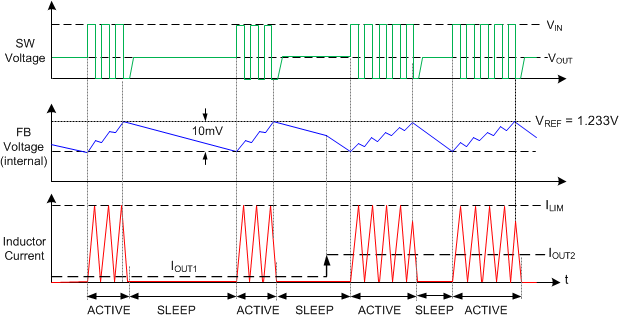 Figure 41. PFM Mode Output Voltage and Inductor Current Representative Waveforms
When operating in PFM mode at given input and output voltages, the chosen filter inductance dictates the PFM pulse frequency as

where
- IPK(PFM) is one of the programmable levels for peak current limit. See Adjustable Current Limit for more detail.
One of the supported ILIM settings enables a function that modulates the peak current threshold levels during the first three switching cycles of each active period as illustrated in Figure 42. This function improves efficiency under most application conditions at the expense of slightly degraded load transient response.
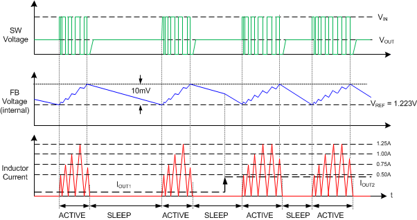 Figure 42. PFM Mode With Modulated ILIM, Output Voltage and Inductor Current Representative Waveforms
As expected, the choice of mode and switching frequency represents a compromise between conversion efficiency, quiescent current, and passive component size. Lower switching frequency implies reduced switching losses (including gate charge losses, transition losses, and so forth) and higher overall efficiency. Higher switching frequency, on the other hand, implies smaller LC output filter and hence, a more compact design. Lower inductance also helps transient response and reduces the inductor DCR conduction loss. The ideal switching frequency in a given application is a tradeoff and thus is determined on a case-by-case basis. It relates to the input voltage, output voltage, most frequent load current level(s), external component choices, and circuit size requirement. At light loads, the PFM converter has a relatively longer sleep time interval and thus operates at lower input quiescent current levels.
7.3.2.2 COT Mode Operation
In COT mode, the LM5166-based converter turns on the high-side MOSFET with constant on-time that adapts to VIN, as defined by Equation 2, to operate with nearly fixed switching frequency when in continuous conduction mode (CCM). The high-side MOSFET turns on when the feedback voltage (VFB) falls below the reference voltage. The regulator control loop maintains a constant output voltage by adjusting the PWM off-time as defined with Equation 3. For stable operation, the feedback voltage must decrease monotonically in phase with the inductor current during the off-time as explained in Ripple Generation Methods.

Diode emulation mode (DEM) prevents negative inductor current, and pulse skipping maintains high efficiency at light load currents by decreasing the effective switching frequency. The COT-controlled LM5166 waveforms in CCM and DEM are shown in Figure 43.
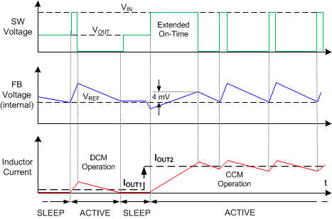 Figure 43. COT Mode Feedback Voltage and Inductor Current Representative Waveforms
The required on-time adjust resistance for a particular frequency (in CCM) is given in Equation 4 and tabulated in Table 1. The maximum programmable on-time is 15 µs.

Table 1. On-Time Adjust Resistance (E96 EIA Values) for Various Switching Frequencies and Output Voltages(1)
| FSW (kHz) | RRT (kΩ) | |||
|---|---|---|---|---|
| VOUT = 1.8 V | VOUT = 3.3 V | VOUT = 5 V | VOUT = 12 V | |
| 100 | 102 | 187 | 287 | 681 |
| 200 | 51.1 | 95.3 | 143 | 340 |
| 300 | 34 | 63.4 | 95.3 | 226 |
| 400 | 25.5 | 47.5 | 71.5 | 169 |
| 500 | 20.5 | 37.4 | 57.6 | 137 |
| 600 | 16.9 | 31.6 | 47.5 | 115 |
7.3.2.2.1 Ripple Generation Methods
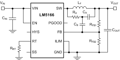
In the Constant-On-Time (COT) control scheme, the on-time is terminated by a one-shot, and the off-time is terminated by the feedback voltage (VFB) falling below the reference voltage (VFB1). Therefore, for stable operation, the feedback voltage must decrease monotonically in phase with the inductor current during the off-time. Furthermore, this change in feedback voltage (VFB) during the off-time must be large enough to dominate any noise present at the feedback node.
Table 2. Ripple Generation Methods
| TYPE | SCHEMATIC | CALCULATION |
| Type 1
Lowest Cost |
 |
Equation 5.

Equation 6.
 |
| Type 2
Reduced Ripple |
 |
Equation 7.

Equation 8.

Equation 9.
 |
| Type 3(1)
Lowest Ripple |
 |
Equation 10.

Equation 11.

Equation 12.
 |
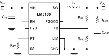
Table 2 presents three different methods for generating appropriate voltage ripple at the feedback node. Type 1 ripple generation method uses a single resistor, designated RESR, in series with the output capacitor. The generated voltage ripple has two components:
- Capacitive ripple caused by the inductor ripple current charging and discharging the output capacitor.
- Resistive ripple caused by the inductor ripple current flowing in the output capacitor ESR and series resistance RESR.
The capacitive ripple component is out of phase with the inductor current. As a result, the capacitive ripple does not decrease monotonically during the off-time. The resistive ripple component is in phase with the inductor current and decreases monotonically during the off-time. The resistive ripple must exceed the capacitive ripple at the output (VOUT) for stable operation. If this condition is not satisfied, unstable switching behavior is observed in COT converters, with multiple on-time bursts in close succession followed by a long off-time. Equation 5 and Equation 6 define the value of the RESR resistor that ensures the required amplitude and phase of the ripple at the feedback node.
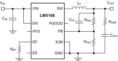
Type-2 ripple generation method uses a CFF capacitor in addition to the RESR resistor. As the output voltage ripple is directly AC-coupled by CFF to the feedback node, the RESR value and ultimately the output voltage ripple are reduced by a factor of VOUT / VFB1.
Type-3 ripple generation method uses an RC network consisting of RA and CA, and the switch node (SW) voltage to generate a triangular ramp. This triangular ramp is then AC-coupled into the feedback node (FB) with capacitor CB. Because this circuit does not use the output voltage ripple, it is suited for applications where low output voltage ripple is critical. Application note AN-1481 Controlling Output Ripple & Achieving ESR Independence in Constant On-Time Regulator Designs provides additional details on this topic.
7.3.2.2.2 COT Mode Light-Load Operation
Diode emulation mode (DEM) operation occurs when the low-side MOSFET switches off as the inductor valley current reaches zero. Here, the load current is less than half of the peak-to-peak inductor current ripple in CCM. Turning off the low-side MOSFET at zero current reduces switching loss, and preventing negative current conduction reduces conduction loss. In DEM, the duration that both high-side and low-side MOSFETs remain off progressively increases as load current decreases.
7.3.3 Low Dropout Operation and 100% Duty Cycle Mode
Using RDSON1 and RDSON2 for the high-side and low-side MOSFET on-state resistances, respectively, and RDCR for the inductor DC resistance, the duty cycle in COT (CCM) or PFM mode is given by Equation 13.

The LM5166 provides a low input voltage to output voltage dropout by engaging the high-side MOSFET at 100% duty cycle. In COT operation, the extended on-time mode seamlessly increases the duty cycle during low dropout conditions or load-step transients. The buck switch on-time extends based on the requirement that the FB voltage exceeds the internal 4-mV FB comparator hysteresis during any COT mode on-time. The on-time (and duty cycle) are extended as needed at low input voltage conditions until the FB voltage reaches the upper threshold. 100% duty cycle operation is eventually reached as the input voltage decreases to a level near the output voltage setpoint. Very low dropout voltages can be achieved with 100% duty cycle and a low DCR inductor.
Note that PFM mode operation provides a natural transition to 100% duty cycle if needed during low input voltage conditions. If the input-to-output voltage difference is very low, the inductor current increases to a level determined by the load and may not reach the peak current threshold required to turn off the buck switch.
Use Equation 14 to calculate the minimum input voltage to maintain output regulation at 100% duty cycle.

7.3.4 Adjustable Output Voltage (FB)
Three voltage feedback settings are available. The fixed 3.3-V and 5-V versions include internal feedback resistors that sense the output directly through the VOUT pin, and the adjustable voltage option senses the output through an external resistor divider connected from the output to the FB pin.
The LM5166 voltage regulation loop regulates the output voltage by maintaining the FB voltage equal to the internal reference voltage (VFB1). A resistor divider programs the ratio from output voltage VOUT to FB. For a target VOUT setpoint, calculate RFB2 based on the selected RFB1 by Equation 15.

RFB1 in the range of 100 kΩ to 1 MΩ is recommended for most applications. A larger RFB1 consumes less DC current, which is necessary if light-load efficiency is critical. However, RFB1 larger than 1 MΩ is not recommended as the feedback path becomes more susceptible to noise. Larger feedback resistances generally require more careful feedback path PCB layout. It is important to route the feedback trace away from the noisy area of the PCB. For more PCB layout recommendations, see Layout.
7.3.5 Adjustable Current Limit
The LM5166 protects the system from overload conditions using cycle-by-cycle current limiting of the peak inductor current. The current sensed in the high-side MOSFET is compared to the current limit threshold set by the ILIM pin (see Table 3). Current is sensed after a 120-ns leading-edge blanking time following the high-side MOSFET turnon. The propagation delay of the current limit comparator is 80 ns, typical.
Table 3. Current Limit Thresholds
| MODE OF OPERATION | RILIM (kΩ) | TYPICAL IHS_LIM (mA) | TYPICAL ILS_LIM (mA) | IOUT(max) (mA) |
|---|---|---|---|---|
| COT Mode | 0 | 750 | 415 | 500 |
| ≥ 100(2) | 500 | 315 | 300 | |
| PFM Mode | 0 | 1250 | N/A | 500 |
| 24.9 | 1250(1) | N/A | 500 | |
| 56.2 | 750 | N/A | 300 | |
| ≥ 100(2) | 500 | N/A | 200 |
Note that in PFM mode, the inductor current ramps from zero to the chosen peak threshold every switching cycle. Consequently, the maximum output current is equal to half the peak inductor current. The output current capability in COT mode is higher and equal to the peak current threshold minus one-half the inductor ripple current. The ripple current is determined by the input and output voltages and the chosen inductance and switching frequency.
7.3.6 Precision Enable (EN) and Hysteresis (HYS)
The precision EN input supports adjustable input undervoltage lockout (UVLO) with hysteresis programmed independently through the HYS pin for application specific power-up and power-down requirements. EN connects to the input of a comparator with 76-mV hysteresis. The reference input of the comparator is connected to a 1.22-V bandgap reference. An external logic signal can be used to drive EN input to toggle the output on and off for system sequencing or protection. The simplest way to enable operation is to connect EN directly to VIN. This allows self-start-up of the LM5166 when VIN is within its valid operating range.
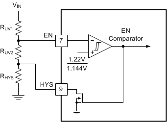 Figure 44. Input Voltage UVLO Using EN and HYS
However, many applications benefit from using a resistor divider RUV1 and RUV2 as shown in Figure 44 to establish a precision UVLO level. Adding RHYS and the connection to the HYS pin increases the voltage hysteresis as needed.
The input UVLO voltages are calculated using Equation 16 and Equation 17.


The LM5166 enters a low IQ shutdown mode when EN is pulled below an NPN transistor base-emitter voltage drop (approximately 0.6 V at room temperature). If EN is below this hard shutdown threshold, the internal LDO regulator powers off and the internal bias supply rail collapses, turning off the bias currents of the LM5166.
7.3.7 Power Good (PGOOD)
The LM5166 has a built-in PGOOD flag to indicate whether the output voltage is within a regulation window. The PGOOD signal can be used for start-up sequencing of downstream converters, as shown in Figure 45, or fault protection. PGOOD is an open-drain output that requires a pullup resistor to a DC supply (12 V maximum). Typical range of pullup resistance is 10 kΩ to 100 kΩ. If necessary, use a resistor divider to decrease the PGOOD pin voltage from a higher pullup rail.
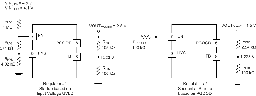 Figure 45. Master-Slave Sequencing Implementation Using PGOOD and EN
When the FB voltage exceeds 94% of the internal reference VFB1, the PGOOD switch turns off and PGOOD will be pulled high. If the FB voltage falls below 87% of VFB1, the PGOOD switch turns on, and PGOOD pulls low to indicate power bad. The rising edge of PGOOD has a built-in noise filter delay of 5 µs.
7.3.8 Configurable Soft Start (SS)
The LM5166 has a flexible and easy-to-use start-up control through the SS pin. A soft-start feature prevents inrush current impacting the LM5166 and its supply when power is first applied. Soft start is achieved by slowly ramping up the target regulation voltage when the device is enabled or powered up. Selectable and adjustable soft-start timing options include minimum delay (no soft-start), 900-µs internally fixed soft-start, and an externally-adjustable soft start.
The simplest way to use the LM5166 is to leave the SS pin open circuit for a 900-µs soft-start time. The LM5166 will employ the internal soft-start control ramp and start-up to the regulated output voltage. In applications with a large amount of output capacitors, higher VOUT, or other special requirements, extend the soft-start time by connecting an external capacitor CSS from SS to GND. Longer soft-start time further reduces the supply current needed to charge the output capacitors. An internal current source (ISS = 10 µA) charges CSS and generates a ramp to control the ramp rate of the output voltage. For a desired soft-start time tSS, the CSS capacitance is:

CSS is discharged by an internal 80-Ω FET when VOUT is shutdown by EN, UVLO, or thermal shutdown.
It is desirable in some applications for the output voltage to reach its nominal setpoint in the shortest possible time. Connecting a 100-kΩ resistor from SS to GND disables the soft-start circuit of the LM5166, and the LM5166 operates in current limit during start-up to rapidly charge the output capacitance.
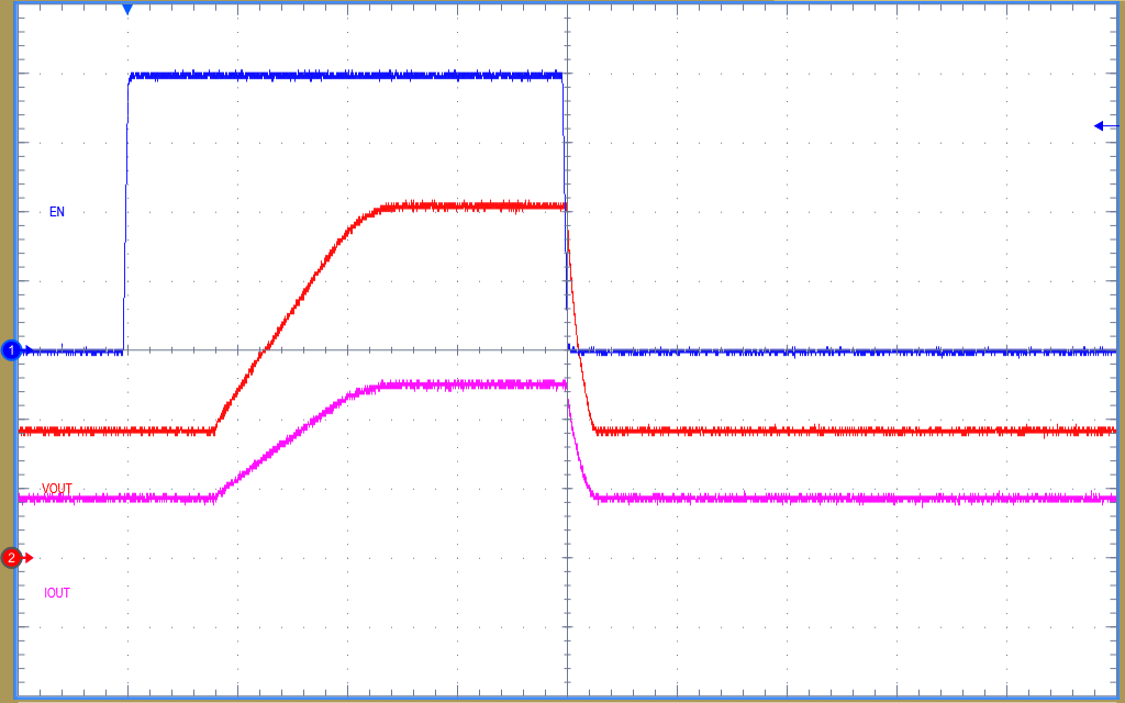
Diode emulation mode (DEM) of the LM5166 prevents negative inductor current enabling monotonic start-up under prebiased output conditions. With a prebiased output voltage, the LM5166 waits until the soft-start ramp allows regulation above the prebiased voltage and then follows the soft-start ramp to the regulation setpoint as shown in Figure 46 and Figure 47.
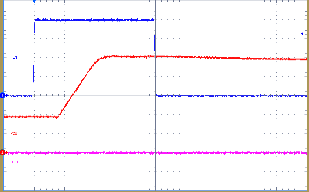
| Time Scale: 2 ms/Div CH1: VEN, 1 V/Div |
CH2: VOUT, 1 V/Div CH4: IOUT, 200 mA/Div |
Figure 52 Circuit, VIN = 24 V, No Load
| Time Scale: 2 ms/Div CH1: VEN, 5 V/Div |
CH2: VOUT, 1 V/Div CH4: IOUT, 200 mA/Div |
Figure 52 Circuit, VIN = 24 V, 500 mA Load
7.3.9 Short-Circuit Operation
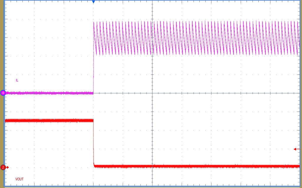
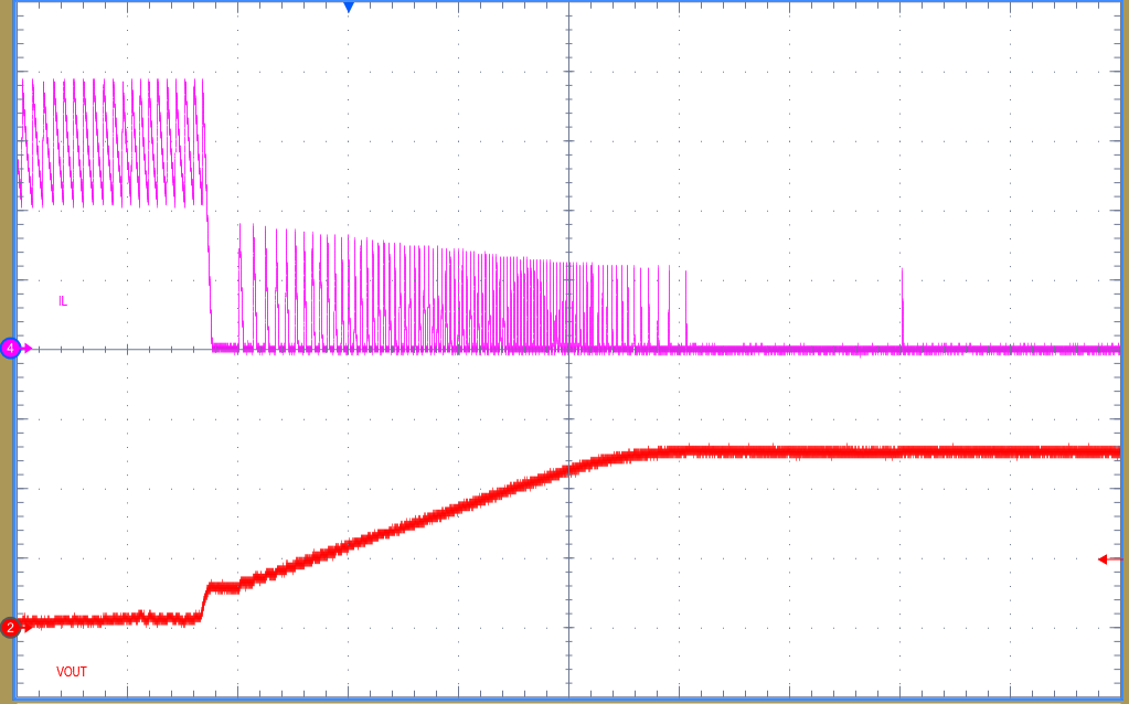
The LM5166 features a clamping circuit that clamps the SS voltage about 175 mV above the FB voltage (see Figure 48 and Figure 49). The circuit is enabled in COT mode and only works when an external soft-start capacitor is connected.
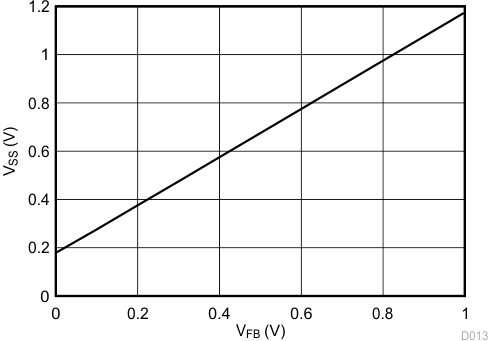
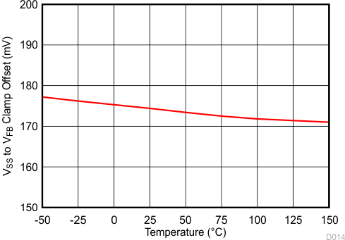
In case of an overload event such as an output short circuit, the clamping circuit discharges the soft-start capacitor. When the short is removed, the FB voltage quickly rises until it reaches the level of the SS pin. Then, the recovery continues under the soft-start capacitor control. Figure 50 and Figure 51 show short-circuit entry and recovery waveforms.
7.3.10 Thermal Shutdown
Thermal shutdown is a built-in self protection to limit junction temperature and prevent damage related to overheating. Thermal shutdown turns off the device when the junction temperature exceeds 170°C typically to prevent further power dissipation and temperature rise. Junction temperature decreases during thermal shutdown, and the LM5166 restarts when the junction temperature falls to 160°C.
7.4 Device Functional Modes
7.4.1 Shutdown Mode
The EN pin provides ON / OFF control for the LM5166. When VEN is below 0.3 V, the device is in shutdown mode. Both the internal LDO and the switching regulator are off. The quiescent current in shutdown mode drops to 4 µA (typical) at VIN = 12 V. The LM5166 also includes undervoltage protection of the internal bias LDO. If the internal bias supply voltage is below the UV threshold level, the switching regulator remains off.
7.4.2 Standby Mode
The internal bias LDO has a lower enable threshold than the switching regulator. When VEN is above 0.6 V and below the precision enable threshold (1.22 V typically), the internal LDO is on and regulating. The precision enable circuitry is turned on if the LDO output is above the bias rail UV threshold. The switching action and output voltage regulation are disabled in the standby mode.
7.4.3 Active Mode – COT
The LM5166 is in active mode when VEN is above the precision enable threshold and the internal bias rail is above its UV threshold level. In COT active mode, the LM5166 operates in one of three modes depending on the load current:
- CCM with fixed switching frequency when the load current is more than half of the peak-to-peak inductor current ripple;
- Pulse skipping and diode emulation mode when load current is less than half of the peak-to-peak inductor current ripple of CCM operation;
- Extended on-time mode when VIN is nearly equal to VOUT (dropout) and during load step transients.
7.4.4 Sleep Mode – COT
The LM5166 is in COT sleep mode when VEN and VIN are above their relevant threshold levels, FB has exceeded its upper hysteresis level, and the output capacitor is sourcing the load current. In COT sleep mode, the LM5166 operates with very low quiescent current (9.7 µA typical). There is a 2-µs wake-up delay from sleep to active modes.
7.4.5 Active Mode – PFM
The LM5166 is in PFM active mode when VEN and VIN are above their relevant thresholds, FB has fallen below the lower hysteresis level, and boundary conduction mode switching is recharging the output capacitor to the upper hysteresis level.
7.4.6 Sleep Mode – PFM
The LM5166 is in PFM sleep mode when VEN and VIN are above their relevant threshold levels, FB has exceeded the upper hysteresis level, and the output capacitor is sourcing the load current. In PFM sleep mode, the LM5166 operates with very low quiescent current (9.7 µA typical). There is a 2-µs wake-up delay from sleep to active modes.
