JAJSIM2 February   2020 LM60430-Q1 , LM60440-Q1

ADVANCE INFORMATION for pre-production products; subject to change without notice.  

  1. 特長
  2. アプリケーション
  3. 概要
    1.     Device Images
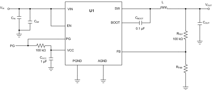
      1.      概略回路図
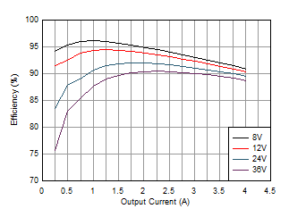
      2.      効率と出力電流との関係 VOUT = 5V、400kHz
  4. 改訂履歴
  5. Device Comparison Table
  6. Pin Configuration and Functions
    1.     Pin Functions
  7. Specifications
    1. 7.1 Absolute Maximum Ratings
    2. 7.2 ESD Ratings
    3. 7.3 Recommended Operating Conditions
    4. 7.4 Thermal Information
    5. 7.5 Electrical Characteristics
    6. 7.6 Timing Characteristics
    7. 7.7 System Characteristics
  8. Detailed Description
    1. 8.1 Overview
    2. 8.2 Functional Block Diagram
    3. 8.3 Feature Description
      1. 8.3.1 Power-Good Flag Output
      2. 8.3.2 Enable and Start-up
      3. 8.3.3 Current Limit and Short Circuit
      4. 8.3.4 Undervoltage Lockout and Thermal Shutdown
    4. 8.4 Device Functional Modes
      1. 8.4.1 Auto Mode
      2. 8.4.2 Dropout
      3. 8.4.3 Minimum Switch On-Time
  9. Application and Implementation
    1. 9.1 Application Information
    2. 9.2 Typical Application
      1. 9.2.1 Design Requirements
      2. 9.2.2 Detailed Design Procedure
        1. 9.2.2.1  Choosing the Switching Frequency
        2. 9.2.2.2  Setting the Output Voltage
        3. 9.2.2.3  Inductor Selection
        4. 9.2.2.4  Output Capacitor Selection
        5. 9.2.2.5  Input Capacitor Selection
        6. 9.2.2.6  CBOOT
        7. 9.2.2.7  VCC
        8. 9.2.2.8  CFF Selection
        9. 9.2.2.9  External UVLO
        10. 9.2.2.10 Maximum Ambient Temperature
      3. 9.2.3 Application Curves
    3. 9.3 EMI
    4. 9.4 What to Do and What Not to Do
  10. 10Power Supply Recommendations
  11. 11Layout
    1. 11.1 Layout Guidelines
      1. 11.1.1 Ground and Thermal Considerations
    2. 11.2 Layout Example
  12. 12デバイスおよびドキュメントのサポート
    1. 12.1 デバイス・サポート
      1. 12.1.1 開発サポート
        1. 12.1.1.1 WEBENCH®ツールによるカスタム設計
    2. 12.2 ドキュメントのサポート
      1. 12.2.1 関連資料
    3. 12.3 ドキュメントの更新通知を受け取る方法
    4. 12.4 サポート・リソース
    5. 12.5 商標
    6. 12.6 静電気放電に関する注意事項
    7. 12.7 Glossary
  13. 13メカニカル、パッケージ、および注文情報

パッケージ・オプション

メカニカル・データ(パッケージ|ピン)
サーマルパッド・メカニカル・データ
発注情報

Application Curves

Unless otherwise specified the following conditions apply: VIN = 12 V, TA = 25°C. The circuit is shown in Figure 17, with the appropriate BOM from Table 4.
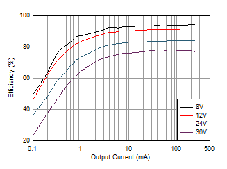
LM60440-Q1 LM60430-Q1 Eff_5Vout_Low_load_PR.gif
VOUT = 5 V 400 kHz
Figure 11. Low-Load Efficiency
LM60440-Q1 LM60430-Q1 LoadReg_PR.gif
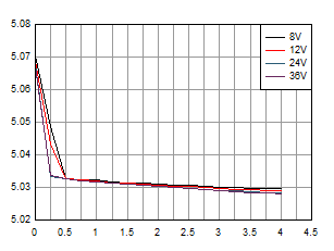
VOUT = 5 V
Figure 13. Line and Load Regulation
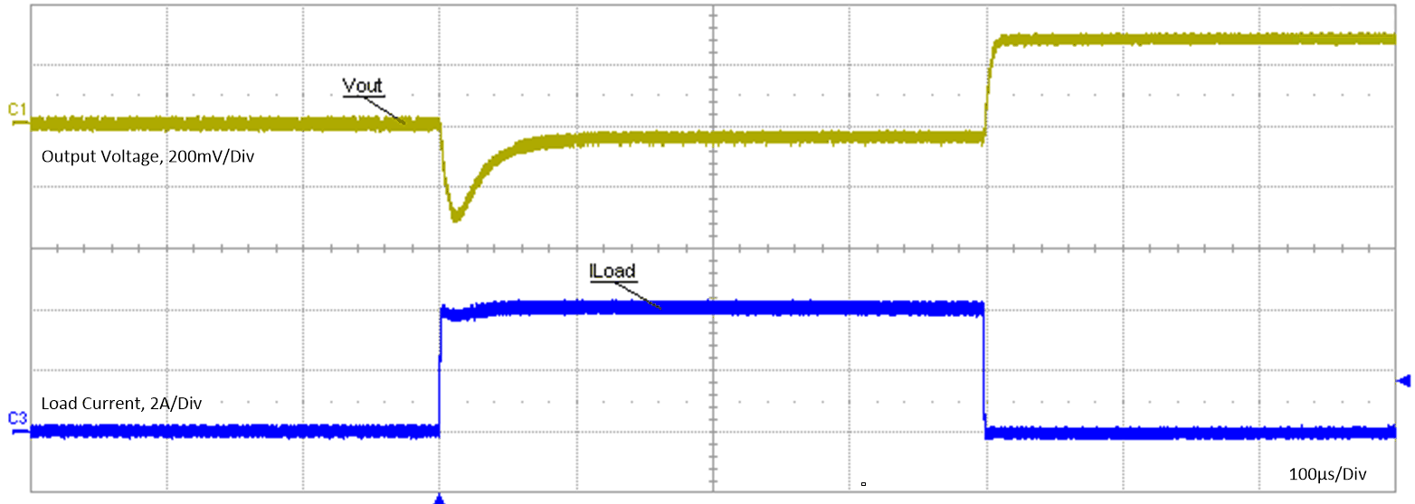
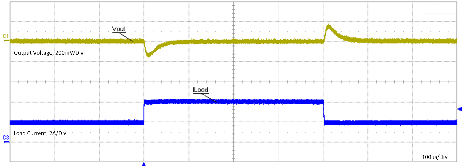
LM60440-Q1 LM60430-Q1 Load_transient_0_to_4A_PR.gif
VIN = 12 V VOUT = 5 V
IOUT = 0 A to 4 A tf = tr = 4 µs
Figure 15. Load Transient
LM60440-Q1 LM60430-Q1 Eff_5Vout_HighLoad_PR.gif
VOUT = 5 V 400 kHz
Figure 12. High-Load Efficiency
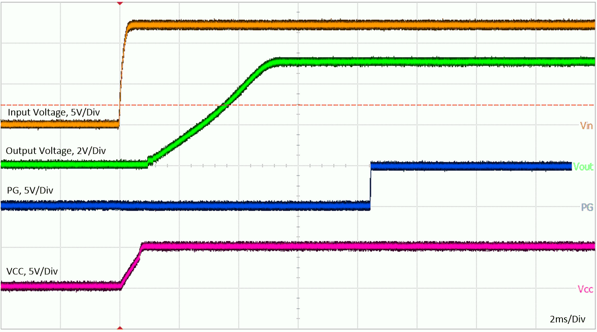
LM60440-Q1 LM60430-Q1 startup_4A_PR.gif
VIN = 13.5 V VOUT = 5 V IOUT = 4 A
Figure 14. Start-up
LM60440-Q1 LM60430-Q1 Load_transient_2_to_4A_PR.gif
VIN = 12 V VOUT = 5 V
tf = tr = 2 µs IOUT = 2 A to 4 A
Figure 16. Load Transient
LM60440-Q1 LM60430-Q1 typ_app_char_cir5.gifFigure 17. Circuit for Application Curves

Table 4. BOM for Typical Application Curves

VOUT FREQUENCY RFBB COUT CIN + CHF L U1
5 V 400 kHz 24.9 k 2 x 47 µF + 22µF 4.7 µF + 2 × 220 nF 6.8 µH, 20.8 mΩ LM60440AQRPKRQ1