JAJSIM1 February   2020 LM60430 , LM60440

ADVANCE INFORMATION for pre-production products; subject to change without notice.  

  1. 特長
  2. アプリケーション
  3. 概要
    1.     Device Images
      1.      概略回路図
      2.      効率と出力電流との関係 VOUT = 5V、400kHz
  4. 改訂履歴
  5. Device Comparison Table
  6. Pin Configuration and Functions
    1.     Pin Functions
  7. Specifications
    1. 7.1 Absolute Maximum Ratings
    2. 7.2 ESD Ratings
    3. 7.3 Recommended Operating Conditions
    4. 7.4 Thermal Information
    5. 7.5 Electrical Characteristics
    6. 7.6 Timing Characteristics
    7. 7.7 System Characteristics
  8. Detailed Description
    1. 8.1 Overview
    2. 8.2 Functional Block Diagram
    3. 8.3 Feature Description
      1. 8.3.1 Power-Good Flag Output
      2. 8.3.2 Enable and Start-up
      3. 8.3.3 Current Limit and Short Circuit
      4. 8.3.4 Undervoltage Lockout and Thermal Shutdown
    4. 8.4 Device Functional Modes
      1. 8.4.1 Auto Mode
      2. 8.4.2 Dropout
      3. 8.4.3 Minimum Switch On-Time
  9. Application and Implementation
    1. 9.1 Application Information
    2. 9.2 Typical Application
      1. 9.2.1 Design Requirements
      2. 9.2.2 Detailed Design Procedure
        1. 9.2.2.1  Choosing the Switching Frequency
        2. 9.2.2.2  Setting the Output Voltage
        3. 9.2.2.3  Inductor Selection
        4. 9.2.2.4  Output Capacitor Selection
        5. 9.2.2.5  Input Capacitor Selection
        6. 9.2.2.6  CBOOT
        7. 9.2.2.7  VCC
        8. 9.2.2.8  CFF Selection
        9. 9.2.2.9  External UVLO
        10. 9.2.2.10 Maximum Ambient Temperature
      3. 9.2.3 Application Curves
    3. 9.3 EMI
    4. 9.4 What to Do and What Not to Do
  10. 10Power Supply Recommendations
  11. 11Layout
    1. 11.1 Layout Guidelines
      1. 11.1.1 Ground and Thermal Considerations
    2. 11.2 Layout Example
  12. 12デバイスおよびドキュメントのサポート
    1. 12.1 デバイス・サポート
      1. 12.1.1 開発サポート
        1. 12.1.1.1 WEBENCH®ツールによるカスタム設計
    2. 12.2 ドキュメントのサポート
      1. 12.2.1 関連資料
    3. 12.3 ドキュメントの更新通知を受け取る方法
    4. 12.4 サポート・リソース
    5. 12.5 商標
    6. 12.6 静電気放電に関する注意事項
    7. 12.7 Glossary
  13. 13メカニカル、パッケージ、および注文情報

パッケージ・オプション

メカニカル・データ(パッケージ|ピン)
サーマルパッド・メカニカル・データ
発注情報

External UVLO

In some cases, an input UVLO level different than that provided internal to the device is needed. This can be accomplished by using the circuit shown in Figure 10. The input voltage at which the device turns on is designated VON; while the turnoff voltage is VOFF. First, a value for RENB is chosen in the range of 10 kΩ to 100 kΩ and then Equation 9 is used to calculate RENT and VOFF.

LM60440 LM60430 EN_uvlo_sch1.gifFigure 10. Setup for External UVLO Application
Equation 9. LM60440 LM60430 EN_uvlo_eq2.gif
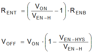
where

  • VON = VIN turnon voltage
  • VOFF = VIN turnoff voltage