JAJSJ65B May 2020 – June 2021 LM62435-Q1
PRODUCTION DATA
- 1 特長
- 2 アプリケーション
- 3 概要
- 4 Revision History
- 5 Device Comparison Table
- 6 Pin Configuration and Functions
- 7 Specifications
-
8 Detailed Description
- 8.1 Overview
- 8.2 Functional Block Diagram
- 8.3
Feature Description
- 8.3.1 EN Uses for Enable and VIN UVLO
- 8.3.2 MODE/SYNC Pin Operation
- 8.3.3 PGOOD Output Operation
- 8.3.4 Internal LDO, VCC UVLO, and BIAS Input
- 8.3.5 Bootstrap Voltage and VCBOOT-UVLO (CBOOT Pin)
- 8.3.6 Adjustable SW Node Slew Rate
- 8.3.7 Spread Spectrum
- 8.3.8 Soft Start and Recovery From Dropout
- 8.3.9 Output Voltage Setting
- 8.3.10 Overcurrent and Short Circuit Protection
- 8.3.11 Thermal Shutdown
- 8.3.12 Input Supply Current
- 8.4 Device Functional Modes
- 9 Application and Implementation
- 10Power Supply Recommendations
- 11Layout
- 12Device and Documentation Support
- 13Mechanical, Packaging, and Orderable Information
8.3.2.1 Level-Dependent MODE/SYNC Pin Control
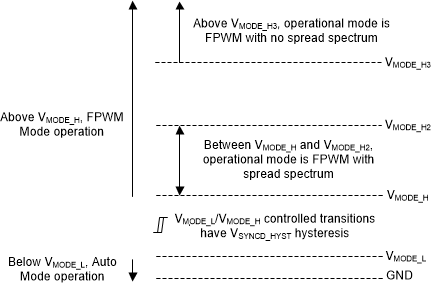
If only a single mode is used, the part can be configured using level-dependent control. Note that the LMQ6235-Q1 cannot be synchronized to an external clock signal in level-dependent mode. Table 8-1 shows a summary of level-dependent mode selection settings. The level-dependent mode selection setting registers after tMODE. The level-dependent mode summary is also depicted in Figure 8-2.
| MODE/SYNC INPUT | MODE |
|---|---|
| GND | Auto Mode with Spread Spectrum |
| VCC OR > VMODE_H AND < VMODE_H2 | FPWM Mode with Spread Spectrum |
| VIN OR > VMODE_H3 | FPWM Mode without Spread Spectrum |
 Figure 8-2 Level-Dependent Mode Selection
Settings
Figure 8-2 Level-Dependent Mode Selection
SettingsNote that during dropout operation, the input voltage is close to VCC. Since this condition is typically seen while operating in dropout, frequency is typically folded back and spread spectrum is deactivated. When VIN increases and the device is no longer in frequency foldback, spread spectrum is reactivated. When the input voltage is between 3 V to 3.7 V and the LMQ6235-Q1 is not in dropout operation, the spread spectrum operation is not guaranteed.
One purpose of level-dependent MODE/SYNC pin control is to dynamically change between FPWM and Auto Mode. To ensure the resistance from MODE/SYNC to ground is < RSYNC_L, it is recommended to use 6 kΩ to ground. The MODE/SYNC pin can then be toggled between FPWM and Auto Mode as shown in Table 8-1.
If Auto Mode without spread spectrum operation is desired, tie the MODE/SYNC pin to ground through a 100-kΩ resistor. Auto Mode without spread spectrum is a fixed option, and the mode cannot be changed dynamically.