SNOS926F May 1999 – September 2014 LM7372
PRODUCTION DATA.
- 1 Features
- 2 Applications
- 3 Description
- 4 Revision History
- 5 Pin Configuration and Functions
- 6 Specifications
- 7 Typical Performance Characteristics
- 8 Detailed Description
- 9 Application and Implementation
- 10Power Supply Recommendations
- 11Layout
- 12Device and Documentation Support
- 13Mechanical, Packaging, and Orderable Information
パッケージ・オプション
デバイスごとのパッケージ図は、PDF版データシートをご参照ください。
メカニカル・データ(パッケージ|ピン)
- DDA|8
- D|16
サーマルパッド・メカニカル・データ
- DDA|8
発注情報
5 Pin Configuration and Functions
NOTE
For SO PowerPAD package the exposed pad should be tied either to V− or left electrically floating. Die attach material is conductive and is internally tied to V−.
8-Pin SO PowerPAD
Package DDA
Top View
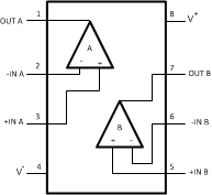
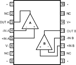
Pin Functions
| PIN | I/O | DESCRIPTION | ||
|---|---|---|---|---|
| NAME | NUMBER | |||
| DDA | D | |||
| * | –– | 1,8,9,16 | –– | Heatsink Pin |
| -IN A | 2 | 4 | I | ChA Inverting Input |
| +IN A | 3 | 5 | I | ChA Non-inverting Input |
| -IN B | 6 | 12 | I | ChB Inverting Input |
| +IN B | 5 | 11 | I | ChB Non-inverting Input |
| NC | –– | 2, 7, 10, 15 | –– | No Connection |
| OUT A | 1 | 3 | O | Output A |
| OUT B | 7 | 13 | O | Output B |
| V- | 4 | 6 | I | Negative Supply |
| V+ | 8 | 14 | I | Positive Supply |