JAJSDD9 June   2017 LM741-MIL

PRODUCTION DATA.  

  1. 特長
  2. アプリケーション
  3. 概要
  4. 改訂履歴
  5. Pin Configuration and Functions
  6. Specifications
    1. 6.1 Absolute Maximum Ratings
    2. 6.2 ESD Ratings
    3. 6.3 Recommended Operating Conditions
    4. 6.4 Thermal Information
    5. 6.5 Electrical Characteristics
  7. Detailed Description
    1. 7.1 Overview
    2. 7.2 Functional Block Diagram
    3. 7.3 Feature Description
      1. 7.3.1 Overload Protection
      2. 7.3.2 Latch-up Prevention
      3. 7.3.3 Pin-to-Pin Capability
    4. 7.4 Device Functional Modes
      1. 7.4.1 Open-Loop Amplifier
      2. 7.4.2 Closed-Loop Amplifier
  8. Application and Implementation
    1. 8.1 Application Information
    2. 8.2 Typical Application
      1. 8.2.1 Design Requirements
      2. 8.2.2 Detailed Design Procedure
      3. 8.2.3 Application Curve
  9. Power Supply Recommendations
  10. 10Layout
    1. 10.1 Layout Guidelines
    2. 10.2 Layout Example
  11. 11デバイスおよびドキュメントのサポート
    1. 11.1 ドキュメントの更新通知を受け取る方法
    2. 11.2 コミュニティ・リソース
    3. 11.3 商標
    4. 11.4 静電気放電に関する注意事項
    5. 11.5 Glossary
  12. 12メカニカル、パッケージ、および注文情報

パッケージ・オプション

メカニカル・データ(パッケージ|ピン)
サーマルパッド・メカニカル・データ
発注情報

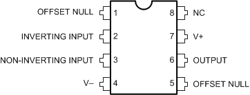
Pin Configuration and Functions


P Package
8-Pin PDIP
Top View
LM741-MIL pinout_p_8_snosd62.gif
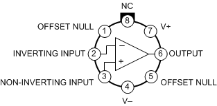
NAB Package
8-Pin CDIP
Top View
LM741-MIL pinout_nab_8_snosd62.gif
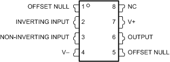
LMC Package
8-Pin TO-99
Top View
LM741-MIL pinout_lmc_8_snosd62.gif

Pin Functions

PIN I/O DESCRIPTION
NAME NO.
INVERTING INPUT 2 I Inverting signal input
NC 8 N/A No Connect, leave floating
NONINVERTING INPUT 3 I Noninverting signal input
OFFSET NULL 1 I Offset null pin used to eliminate the offset voltage and balance the input voltages.
OFFSET NULL 5
OUTPUT 6 O Amplified signal output
V+ 7 I Positive supply voltage
V– 4 I Negative supply voltage