JAJS745D November 1994 – February 2024 LMC6032 , LMC6034
PRODUCTION DATA
- 1
- 1特長
- 2アプリケーション
- 3概要
- 4Pin Configuration and Functions
- 5Specifications
- 6Application and Implementation
- 7Device and Documentation Support
- 8Revision History
- 9Mechanical, Packaging, and Orderable Information
パッケージ・オプション
デバイスごとのパッケージ図は、PDF版データシートをご参照ください。
メカニカル・データ(パッケージ|ピン)
- D|14
サーマルパッド・メカニカル・データ
- D|14
発注情報
Typical Single-Supply Applications
Additional single-supply applications ideas are found in the LM358 data sheet. The LMC603x is pin-for-pin compatible with the LM358 and offers greater bandwidth and input resistance over the LM358. These features can improve the performance of many existing single-supply applications. Be aware, however, the supply voltage range of the LMC603x is smaller than that of the LM358.
 Figure 6-6 Instrumentation Amplifier
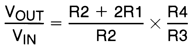
If R1 = R5, R3 = R6, and R4 = R7, then AV = 100 for circuit shown.
Use low-drift resistors for good CMRR performance over temperature. Matching of R3 to R6 and R4 to R7 affects CMRR. Gain is adjusted through R2. CMRR is adjusted through R7. An improved circuit can be designed using the RES11A-Q1, low-drift, precision, matched resistor pairs. Figure 6-7 shows how a precise gain of 99 is easily implemented. The capacitors are optional and are be used to improve noise performance, if needed.
 Figure 6-7 Improved
Instrumentation Amplifier With RES11A
Figure 6-7 Improved
Instrumentation Amplifier With RES11A
fOSC = 1/2πRC
where R = R1 = R2 and C = C1 = C2.
This circuit, as shown, oscillates at 2.0kHz with a peak-to-peak output swing of 4.0V.
 Figure 6-9 Low-Leakage Sample-and-Hold
 Figure 6-11 Power
Amplifier
Figure 6-11 Power
Amplifier") Figure 6-13 1Hz
Low-Pass Filter (Maximally Flat, Dual Supply Only)
Figure 6-13 1Hz
Low-Pass Filter (Maximally Flat, Dual Supply Only) Figure 6-10 1Hz
Square-Wave Oscillator
Figure 6-10 1Hz
Square-Wave Oscillator
| fO = 10Hz, Q = 2.1, gain = −8.8 |

| fc = 10Hz, d = 0.895, gain = 1, 2dB pass-band ripple |

| Gain = −46.8 Output offset voltage reduced to the level of the input offset voltage of the bottom amplifier (typically 1mV). |