JAJSDD7 June 2017 LMC6482-MIL
PRODUCTION DATA.
- 1 特長
- 2 アプリケーション
- 3 概要
- 4 改訂履歴
- 5 Pin Configuration and Functions
- 6 Specifications
- 7 Detailed Description
- 8 Application and Implementation
- 9 Power Supply Recommendations
- 10Layout
- 11デバイスおよびドキュメントのサポート
- 12メカニカル、パッケージ、および注文情報
10 Layout
10.1 Layout Guidelines
It is generally recognized that any circuit which must operate with less than 1000 pA of leakage current requires special layout of the PC board. When one wishes to take advantage of the ultralow input current of the LMC6482-MIL, typically less than 20 fA, it is essential to have an excellent layout. Fortunately, the techniques of obtaining low leakages are quite simple. First, the user must not ignore the surface leakage of the PCB, even through it may sometimes appear acceptably low, because under conditions of high humidity or dust or contamination, the surface leakage will be appreciable.
To minimize the effect of any surface leakage, lay out a ring of foil completely surrounding the LM6482s inputs and the terminals of capacitors, diodes, conductors, resistors, relay terminals, and so forth connected to the inputs of the op-amp, as in Figure 78. To have a significant effect, guard rings should be placed on both the top and bottom of the PCB. This PC foil must then be connected to a voltage which is at the same voltage as the amplifier inputs, because no leakage current can flow between two points at the same potential. For example, a PCB trace-to-pad resistance of 1012 Ω, which is normally considered a very large resistance, could leak 5 pA if the trace were a 5-V bus adjacent to the pad of the input. This would cause a 250 times degradation from the actual performance of the LMC6482-MIL. However, if a guard ring is held within 5 mV of the inputs, then even a resistance of 1011 Ω would cause only 0.05 pA of leakage current. See Figure 79 through Figure 81 for typical connections of guard rings for standard op-amp configurations.
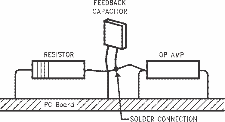
The designer should be aware that when it is inappropriate to lay out a PCB for the sake of just a few circuits, another technique is even better than a guard ring on a PCB: Do not insert the input pin of the amplifier into the PCB at all, but bend it up in the air and use only air as an insulator. Air is an excellent insulator. In this case you may have to forego some of the advantages of PCB construction, but the advantages are sometimes well worth the effort of using point-to-point up-in-the-air wiring. See Figure 82.
10.2 Layout Example
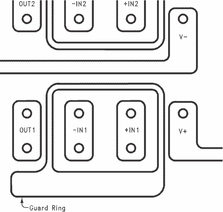 Figure 78. Example of Guard Ring in PCB Layout Typical Connections of Guard Rings
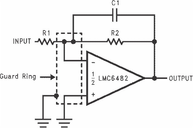 Figure 79. Inverting Amplifier Typical Connections of Guard Rings
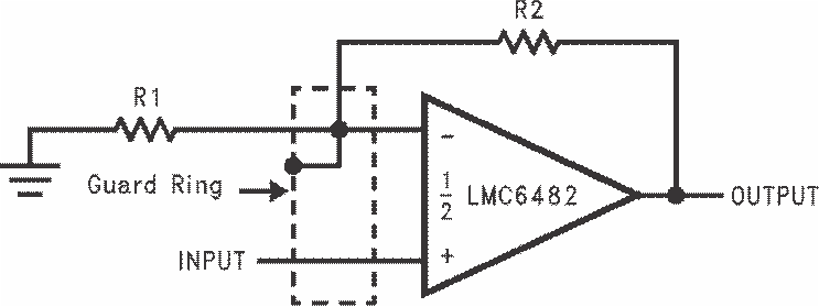 Figure 80. Noninverting Amplifier Typical Connections of Guard Rings
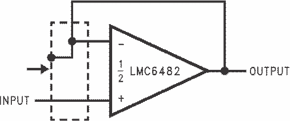 Figure 81. Follower Typical Connections of Guard Rings
