SNLS315H April 2010 – August 2015 LMH0387
PRODUCTION DATA.
- 1 Features
- 2 Applications
- 3 Description
- 4 Revision History
- 5 Pin Configuration and Functions
-
6 Specifications
- 6.1 Absolute Maximum Ratings
- 6.2 ESD Ratings
- 6.3 Recommended Operating Conditions
- 6.4 Thermal Information
- 6.5 Control Pin Electrical Characteristics
- 6.6 Input Mode (Equalizer) DC Electrical Characteristics
- 6.7 Output Mode (Cable Driver) DC Electrical Characteristics
- 6.8 Input Mode (Equalizer) AC Electrical Characteristics
- 6.9 Output Mode (Cable Driver) AC Electrical Characteristics
- 6.10 Input Mode (Equalizer) SPI Interface AC Electrical Characteristics
- 6.11 Typical Characteristics
-
7 Detailed Description
- 7.1 Overview
- 7.2 Functional Block Diagram
- 7.3 Feature Description
- 7.4 Device Functional Modes
- 7.5 Programming
- 7.6 Register Maps
- 8 Application and Implementation
- 9 Power Supply Recommendations
- 10Layout
- 11Device and Documentation Support
- 12Mechanical, Packaging, and Orderable Information
7 Detailed Description
7.1 Overview
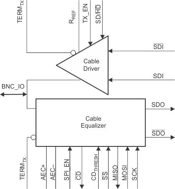
The LMH0387 3 Gbps HD/SD SDI Configurable I/O Adaptive Cable Equalizer / Cable Driver provides a single chip interface to a BNC. The same I/O pin is used both for the input and the output functions of the device, allowing the system designer to use a BNC attached to the device as either an input or an output. The LMH0387 operates over a wide range of data rates from 125 Mbps to 2.97 Gbps and supports ST 424, ST 292, ST 344, ST 259, and DVB/ASI standards. The LMH0387 includes passive components for the return loss network – simplifying board design and development time.
7.2 Functional Block Diagram

7.3 Feature Description
The LMH0387 can be configured either in the input mode as an equalizer to receive data over coaxial cable or in the output mode as a cable driver to transmit data over coaxial cable. The LMH0387 requires register programming to operate either in Input Mode (Equalizer) or Output Mode (Cable Driver).
7.3.1 Input Mode (Equalizer) Description
SPI register access is required while operating the LMH0387 in the input mode. The equalizer launch amplitude fine tuning must be set to nominal through the SPI for correct equalizer operation. To do this, write 30h (“00110000 binary”) to SPI register 02h. The SPI registers provide access to many other useful LMH0387 features while in the input mode. Refer to the Input Mode (Equalizer) SPI Register Access section for details.
7.3.1.1 Input Interfacing
The LMH0387 accepts a single-ended input at the BNC_IO pin. The input must be AC coupled as shown in Figure 9 . The TERMRX input must be properly terminated with a 1-µF capacitor followed by a 220-Ω resistor to ground.
The LMH0387 BNC_IO input can be optimized for different launch amplitudes through the SPI (see Launch Amplitude Optimization (Register 02h) in the Input Mode (Equalizer) SPI Register Access section).
The LMH0387 correctly handles equalizer pathological signals for standard and high definition serial digital video, as described in ST RP 178 and RP 198, respectively.
7.3.1.2 Output Interfacing
The LMH0387 equalizer outputs, SDO and SDO, are internally terminated 100-Ω LVDS outputs. These outputs can be DC coupled to most common differential receivers.
The default output common mode voltage (VOS) is 1.25 V. The output common mode voltage may be adjusted through the SPI in 200 mV increments, from 1.05 V to 1.85 V (see Output Driver Adjustments (Register 01h) in the Input Mode (Equalizer) SPI Register Access section). This adjustable output common mode voltage offers flexibility for interfacing to many types of receivers.
The default differential output swing (VSSP-P) is 700 mVP-P. The differential output swing may be adjusted through the SPI in 100 mV increments from 400 mVP-P to 800 mVP-P (see Output Driver Adjustments (Register 01h) in the Input Mode (Equalizer) SPI Register Access section).
The LMH0387 equalizer output should be DC coupled to the input of the receiving device as long as the common mode ranges of both devices are compatible. 100-Ω differential transmission lines should be used to connect between the LMH0387 outputs and the input of the receiving device where possible.
The LMH0387 allows flexibility when interfacing to low voltage crosspoint switches (that is, 1.8 V) and other devices with limited input ranges. The LMH0387 equalizer outputs can be DC coupled to these devices in most cases.
The LMH0387 may be AC coupled to the receiving device when necessary. For example, the LMH0387 equalizer outputs are not strictly compatible with 3.3 V CML and thus should not be connected through 50-Ω resistors to 3.3 V. If the input common mode range of the receiving device is not compatible with the output common mode range of the LMH0387, then AC coupling is required. Following the AC coupling capacitors, the signal may have to be biased at the input of the receiving device.
7.3.1.3 Carrier Detect (CD)
Carrier detect CD indicates if a valid signal is present at the LMH0387 BNC_IO pin. If CDTHRESH is used, the carrier detect threshold will be altered accordingly. CD provides a high voltage when no signal is present at the LMH0387 BNC_IO pin. CD is low when a valid input signal is detected.
7.3.1.4 Carrier Detect Threshold (CDTHRESH)
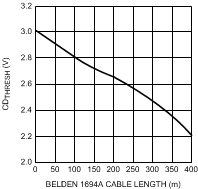
The CDTHRESH pin sets the threshold for the carrier detect. The carrier detect threshold is set by applying a voltage inversely proportional to the length of cable to equalize before loss of carrier is triggered. The applied voltage must be greater than the CDTHRESH floating voltage (typically 1.3 V) to change the CD threshold. As the applied CDTHRESH voltage is increased, the amount of cable that will be equalized before carrier detect is deasserted is decreased. CDTHRESH may be left unconnected or connected to ground for normal CD operation.
Figure 7 shows the minimum CDTHRESH input voltage required to force carrier detect to inactive vs. Belden 1694A cable length. The results shown are valid for Belden 1694A cable lengths of 0 m to 120 m at 2.97 Gbps, 0 m to200 m at 1.485 Gbps, and 0 m to 400 m at 270 Mbps.
 Figure 7. CDTHRESH vs Belden 1694A Cable Length
7.3.1.5 Auto Sleep
The LMH0387 equalizer is set for auto sleep operation by default. The equalizer portion of the LMH0387 powers down when no input signal is detected on the BNC_IO pin. The equalizer powers on again once an input signal is detected. The auto sleep functionality can be changed to force sleep or turned off completely through the SPI registers.
In auto sleep mode, the time to power down the equalizer when the input signal is removed is less than 200 µs and should not have any impact on the system timing requirements. The equalizer will wake up automatically once an input signal is detected, and the delay between signal detection and full functionality of the equalizer is negligible. The overall system will be limited only by the settling time constant of the equalizer adaptation loop.
7.3.2 Output Mode (Cable Driver) Description
7.3.2.1 Input Interfacing
The LMH0387 cable driver accepts differential input signals which can be DC or AC coupled.
7.3.2.2 Output Interfacing
The LMH0387 cable driver uses 75-Ω internally terminated current mode outputs. The output level is 800 mVP-P with an RREF resistor of 715 Ω. The RREF resistor is connected between the RREF pin and VCC, and should be placed as close as possible to the RREF pin.
The output should be AC coupled as shown in the Figure 9. The TERMTX output must be properly terminated with a 4.7-µF capacitor followed by a 75-Ω resistor to ground as shown.
7.3.2.3 Output Slew Rate Control
The LMH0387 cable driver output rise and fall times are selectable for either ST 259 or ST 424 / 292 compliance through the SD/HD pin. For slower rise and fall times, or ST 259 compliance, SD/HD is set high. For faster rise and fall times, or ST 424 and ST 292 compliance, SD/HD is set low. SD/HD has an internal pulldown.
7.3.2.4 Output Enable
The LMH0387 cable driver can be enabled or disabled with the TX_EN pin. When set low, the cable driver is powered off. TX_EN has an internal pullup to enable the cable driver by default. When using the LMH0387 in the input mode (as an equalizer), the cable driver must be disabled by setting the TX_EN pin low.
7.4 Device Functional Modes
SPI register access is required while operating the LMH0387 in the input mode. The equalizer launch amplitude fine tuning must be set to nominal through the SPI for correct equalizer operation. To do this, write 30h (“00110000 binary”) to SPI register 02h. The SPI registers provide access to many other useful LMH0387 features while in the input mode.
To configure the LMH0387 in the output mode, the cable driver must be enabled. The equalizer may either be disabled for power savings or enabled to provide a loopback path for the data being transmitted. For the normal output mode (equalizer disabled for power savings) follow these steps:
- Disable the equalizer by forcing it to sleep through the SPI. To do this, write “10” (force sleep) to bits [4:3] of SPI register 00h.
- Enable the cable driver by pulling the TX_EN pin high.
7.5 Programming
The LMH0387 3 Gbps HD/SD SDI Configurable I/O Adaptive Cable Equalizer / Cable Driver is used at the input or output port of digital video equipment. It is designed to allow the sharing of a single BNC connector for either input or output. The LMH0387 must be configured in either the output mode as a cable driver, or the input mode as an equalizer.
7.5.1 Output Mode (Cable Driver)
To configure the LMH0387 in the output mode, the cable driver must be enabled. The equalizer may either be disabled for power savings or enabled to provide a loopback path for the data being transmitted. For the normal output mode (equalizer disabled for power savings) follow these steps:
- Disable the equalizer by forcing it to sleep through the SPI. To do this, write “10” (force sleep) to bits [4:3] of SPI register 00h.
- Enable the cable driver by pulling the TX_EN pin high.
To configure the LMH0387 for the output mode with the loopback path, the equalizer can be enabled in output mode by writing either “01” (auto sleep – default) or “00” (never sleep) to bits [4:3] of SPI register 00h. In this case, the LMH0387 input/output mode may be configured simply by toggling the TX_EN pin because the equalizer remains active in either mode (TX_EN set low for input mode and high for output mode).
7.5.2 Input Mode (Equalizer)
To configure the LMH0387 in the input mode, the equalizer must be enabled and the cable driver must be disabled as described in the following steps:
- Disable the cable driver by pulling the TX_EN pin low.
- Enable the equalizer by setting the sleep mode through the SPI to either auto sleep or disabled (never sleep). To do this, write either “01” (auto sleep – default) or “00” (never sleep) to bits [4:3] of SPI register 00h.
- Set the equalizer launch amplitude fine tuning to the nominal setting through the SPI. To do this, write 30h (“00110000” binary) to SPI register 02h.
7.5.3 Input Mode (Equalizer) SPI Register Access
SPI register access is required for correct input mode (equalizer) operation. The SPI registers provide access to all of the equalizer features along with a cable length indicator, programmable output common mode voltage and swing, and launch amplitude optimization. There are four supported 8-bit registers in the device (see SPI Registers).
Note: The SPI_EN pin must always be pulled high while using the LMH0387 in the input mode (equalizer), and may optionally be pulled high while using the LMH0387 in the output mode (cable driver) as well.
7.5.3.1 SPI Write
The SPI write is shown in Figure 2. The MOSI payload consists of a “0” (write command), seven address bits, and eight data bits. The SS signal is driven low, and the 16 bits are sent to the LMH0387's MOSI input. Data is latched on the rising edge of SCK. The MISO output is normally tri-stated during this operation. After the SPI write, SS must return high.
7.5.3.2 SPI Read
The SPI read is shown in Figure 3. The MOSI payload consists of a “1” (read command) and seven address bits. The SS signal is driven low, and the eight bits are sent to the LMH0387's MOSI input. The addressed location is accessed immediately after the rising edge of the 8th clock and the eight data bits are shifted out on MISO starting with the falling edge of the 8th clock. MOSI must be tri-stated immediately after the rising edge of the 8th clock. After the SPI read, SS must return high.
7.5.3.3 Output Driver Adjustments (Register 01h)
The equalizer output driver swing (amplitude) and offset voltage (common mode voltage) are adjustable through SPI register 01h.
7.5.3.3.1 Output Swing
The output swing is adjustable through bits [7:5] of SPI register 01h. The default value for these register bits is “011” for a peak-to-peak differential output voltage of 700 mVP-P. The output swing can be adjusted in 100 mV increments from 400 mVP-P to 800 mVP-P.
7.5.3.3.2 Offset Voltage
The offset voltage is adjustable through bits [4:2] of SPI register 01h. The default value for these register bits is “001” for an output offset of 1.25 V. The output common mode voltage may be adjusted in 200 mV increments, from 1.05 V to 1.85 V. It can also be set to “101” for the maximum offset voltage. At this maximum offset voltage setting, the outputs are referenced to the positive supply and the offset voltage is around 2.1 V.
7.5.3.4 Launch Amplitude Optimization (Register 02h)
The LMH0387 can compensate for attenuation of the input signal before the equalizer. This compensation is useful for applications with a passive splitter at the equalizer input or a non-ideal input termination network, and is controlled by SPI register 02h.
NOTE
For correct equalizer operation with the default SMPTE 800 mVP-P launch amplitude and no external attenuation, the equalizer launch amplitude fine tuning must be set to the “nominal” setting through the SPI. To do this, write 30h (“00110000” binary) to SPI register 02h.
7.5.3.4.1 Coarse Control
Bit 7 of SPI register 02h is used for coarse control of the launch amplitude setting. At the default setting of “0”, the equalizer operates normally and expects a launch amplitude of 800 mVP-P. Bit 7 may be set to “1” to optimize the equalizer for input signals with 6 dB of attenuation (400 mVP-P).
7.5.3.4.2 Fine Control
Once the coarse control is set, the equalizer input compensation may be further fine tuned by bits [6:3] of SPI register 02h. These bits may be used to tweak the input gain stage -2% to 60% around the coarse control setting. For typical equalizer operation, bits [6:3] of SPI register 02h should be changed from the default setting of “0000” to the nominal setting of “0110”.
7.5.3.5 Cable Length Indicator (CLI (Register 03h)
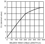
The Cable Length Indicator (CLI) provides an indication of the length of cable attached to the equalizer input. CLI is accessible through bits [7:3] of SPI register 03h. The 5-bit CLI ranges in decimal value from 0 to 25 (“00000” to “11001” binary) and increases as the cable length is increased. Figure 8 shows typical CLI values vs. Belden 1694A cable length. CLI is valid for Belden 1694A cable lengths of 0 m to 120 m at 2.97 Gbps, 0 m to 200 m at 1.485 Gbps, and 0 m to 400 m at 270 Mbps.
 Figure 8. CLI vs. Belden 1694A Cable Length
7.5.4 Input Mode (Equalizer) SPI Register Access
7.5.4.1 General Control (Register 00h)
SPI Register 00h, General Control, provides access to many basic features of the equalizer, including the carrier detect status and the mute, sleep mode, and extended 3G reach mode controls.
7.5.4.1.1 Carrier Detect
This bit shows the status of the carrier detect for the BNC_IO pin.
7.5.4.1.2 Mute
The mute control can be used to manually mute or enable SDO and SDO. Setting this bit to “1” will mute the equalizer outputs by forcing them to logic zero. Setting the mute bit to “0” will force the equalizer outputs to be active.
7.5.4.1.3 Sleep Mode
The sleep mode is used to automatically or selectively power down the equalizer for power savings when it is not needed. The auto sleep mode allows the equalizer to power down when no input signal is detected, and is activated by default or by writing “01” to bits [4:3] of SPI register 00h. If the auto sleep mode is active, the equalizer goes into a deep power save mode when no input signal is detected on the BNC_IO pin. The device powers on again once an input signal is detected. The sleep functionality can be turned off completely (equalizer will never sleep) by writing “00” to bits [4:3] of SPI register 00h. Additionally, the equalizer can be forced to power down regardless of whether there is an input signal or not by writing “10” to bits [4:3] of SPI register 00h. The sleep mode has precedence over the mute mode.
7.5.4.1.4 Extended 3G Reach Mode
The LMH0387 equalizer provides a mode to extend the 3G cable reach in systems that have margin in the jitter budget. This allows for additional cable reach at 2.97 Gbps at the expense of slightly higher output jitter. The extended 3G reach mode provides 10m of additional Belden 1694A cable reach, with an increase of output jitter at this longer cable length of 0.05 to 0.1 UI. (Note: In Extended 3G Reach Mode, the maximum equalizable cable lengths for HD and SD data rates will be limited to less than what can be achieved in normal mode).