SNLS315H April 2010 – August 2015 LMH0387
PRODUCTION DATA.
- 1 Features
- 2 Applications
- 3 Description
- 4 Revision History
- 5 Pin Configuration and Functions
-
6 Specifications
- 6.1 Absolute Maximum Ratings
- 6.2 ESD Ratings
- 6.3 Recommended Operating Conditions
- 6.4 Thermal Information
- 6.5 Control Pin Electrical Characteristics
- 6.6 Input Mode (Equalizer) DC Electrical Characteristics
- 6.7 Output Mode (Cable Driver) DC Electrical Characteristics
- 6.8 Input Mode (Equalizer) AC Electrical Characteristics
- 6.9 Output Mode (Cable Driver) AC Electrical Characteristics
- 6.10 Input Mode (Equalizer) SPI Interface AC Electrical Characteristics
- 6.11 Typical Characteristics
-
7 Detailed Description
- 7.1 Overview
- 7.2 Functional Block Diagram
- 7.3 Feature Description
- 7.4 Device Functional Modes
- 7.5 Programming
- 7.6 Register Maps
- 8 Application and Implementation
- 9 Power Supply Recommendations
- 10Layout
- 11Device and Documentation Support
- 12Mechanical, Packaging, and Orderable Information
10 Layout
10.1 Layout Guidelines
For information on layout and soldering of the laminate TLGA package, refer to the following application note: AN-1125 (SNAA002), Laminate CSP/FBGA.
NOTE
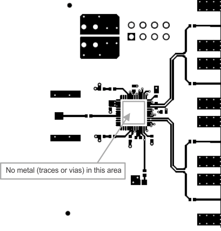
For a CSP package, it is a general requirement not to have any metal (traces or vias) on the top layer in the area directly underneath the device, other than the footprint. This is intended to provide a flat planar surface for the package.
The ST 424, 292, and 259 standards have stringent requirements for the input and output return loss of receivers and transmitters, which essentially specify how closely they must resemble a 75-Ω network. Any non-idealities in the network between the BNC and the LMH0387 will degrade the return loss. Take care to minimize impedance discontinuities both for the BNC footprint and for the trace between the BNC and the LMH0387 to ensure that the characteristic impedance is 75 Ω. Best return loss performance is achieved with the LMH0387 placed closely to the BNC to minimize the trace length between the BNC and the LMH0387's BNC_IO pin. Consider the following PCB recommendations:
- Place the LMH0387 in close proximity to the BNC.
- Use surface mount components, and use the smallest components available. In addition, use the smallest size component pads.
- Select trace widths that minimize the impedance mismatch between the BNC and the LMH0387.
- Select a board stack up that supports both 75-Ω single-ended traces and 100-Ω loosely-coupled differential traces.
- Maintain symmetry on the complementary signals.
- Route 100-Ω traces uniformly (keep trace widths and trace spacing uniform along the trace).
- Avoid sharp bends in the signal path; use 45° or radial bends.
- Place bypass capacitors close to each power pin, and use the shortest path to connect device power and ground pins to the respective power or ground planes.
- Remove ground plane under input/output components to minimize parasitic capacitance.
10.2 Layout Example
 Figure 11. Ground and VCC Relief Under Controlled Impedance Component Pads
 Figure 12. Top Etch Routing Restriction