JAJSI48C March   2017  – October 2019 LMH1228

PRODUCTION DATA.  

  1. 特長
  2. アプリケーション
  3. 概要
    1.     ブロック概略図
  4. 改訂履歴
  5. Pin Configuration and Functions
    1.     Pin Functions
  6. Specifications
    1. 6.1 Absolute Maximum Ratings
    2. 6.2 ESD Ratings
    3. 6.3 Recommended Operating Conditions
    4. 6.4 Thermal Information
    5. 6.5 Electrical Characteristics
    6. 6.6 Recommended SMBus Interface Timing Specifications
    7. 6.7 Serial Parallel Interface (SPI) Timing Specifications
    8. 6.8 Typical Characteristics
  7. Detailed Description
    1. 7.1 Overview
    2. 7.2 Functional Block Diagram
    3. 7.3 Feature Description
      1. 7.3.1 4-Level Input Pins and Thresholds
      2. 7.3.2 OUT0_SEL and SDI_OUT2_SEL Control
      3. 7.3.3 Input Signal Detect
      4. 7.3.4 Continuous Time Linear Equalizer (CTLE)
      5. 7.3.5 Clock and Data (CDR) Recovery
      6. 7.3.6 Internal Eye Opening Monitor (EOM)
      7. 7.3.7 Output Function Control
      8. 7.3.8 Output Driver Control
        1. 7.3.8.1 Line-Side Output Cable Driver (SDI_OUT1+, SDI_OUT2+)
          1. 7.3.8.1.1 Output Amplitude (VOD)
          2. 7.3.8.1.2 Output Pre-Emphasis
          3. 7.3.8.1.3 Output Slew Rate
          4. 7.3.8.1.4 Output Polarity Inversion
        2. 7.3.8.2 Host-Side 100-Ω Output Driver (OUT0±)
      9. 7.3.9 Status Indicators and Interrupts
        1. 7.3.9.1 LOCK_N (Lock Indicator)
        2. 7.3.9.2 SD_N (Signal Detect)
        3. 7.3.9.3 INT_N (Interrupt)
    4. 7.4 Device Functional Modes
      1. 7.4.1 System Management Bus (SMBus) Mode
        1. 7.4.1.1 SMBus Read and Write Transaction
          1. 7.4.1.1.1 SMBus Write Operation Format
          2. 7.4.1.1.2 SMBus Read Operation Format
      2. 7.4.2 Serial Peripheral Interface (SPI) Mode
        1. 7.4.2.1 SPI Read and Write Transactions
        2. 7.4.2.2 SPI Write Transaction Format
        3. 7.4.2.3 SPI Read Transaction Format
        4. 7.4.2.4 SPI Daisy Chain
    5. 7.5 Register Maps
  8. Application and Implementation
    1. 8.1 Application Information
      1. 8.1.1 SMPTE Requirements and Specifications
      2. 8.1.2 Low-Power Optimization
      3. 8.1.3 Optimized Loop Bandwidth Settings for Arria 10 FPGA Applications
    2. 8.2 Typical Applications
      1. 8.2.1 Dual Cable Driver
        1. 8.2.1.1 Design Requirements
        2. 8.2.1.2 Detailed Design Procedure
        3. 8.2.1.3 Application Curves
      2. 8.2.2 Distribution Amplifier
        1. 8.2.2.1 Design Requirements
        2. 8.2.2.2 Detailed Design Procedure
        3. 8.2.2.3 Application Curves
  9. Power Supply Recommendations
  10. 10Layout
    1. 10.1 Layout Guidelines
      1. 10.1.1 Board Stack-Up and Ground References
      2. 10.1.2 High-Speed PCB Trace Routing and Coupling
        1. 10.1.2.1 SDI_OUT1± and SDI_OUT2±:
        2. 10.1.2.2 IN0± and OUT0±:
      3. 10.1.3 Anti-Pads
      4. 10.1.4 BNC Connector Layout and Routing
      5. 10.1.5 Power Supply and Ground Connections
      6. 10.1.6 Footprint Recommendations
    2. 10.2 Layout Example
  11. 11デバイスおよびドキュメントのサポート
    1. 11.1 ドキュメントのサポート
      1. 11.1.1 関連資料
    2. 11.2 ドキュメントの更新通知を受け取る方法
    3. 11.3 サポート・リソース
    4. 11.4 商標
    5. 11.5 静電気放電に関する注意事項
    6. 11.6 輸出管理に関する注意事項
    7. 11.7 Glossary
  12. 12メカニカル、パッケージ、および注文情報
    1. 12.1 Package Option Addendum
      1. 12.1.1 Packaging Information
      2. 12.1.2 Tape and Reel Information

パッケージ・オプション

メカニカル・データ(パッケージ|ピン)
サーマルパッド・メカニカル・データ
発注情報

Power Supply Recommendations

The LMH1228 requires decoupling capacitors to ensure a stable power supply. For power supply decoupling, 0.1-μF surface-mount ceramic capacitors must be placed close to each VDD_CDR, VDD_LDO, and VIN supply pin to VSS. Larger bulk capacitors (for example, 10 μF and 1 μF) are recommended for VDD_CDR and VIN.
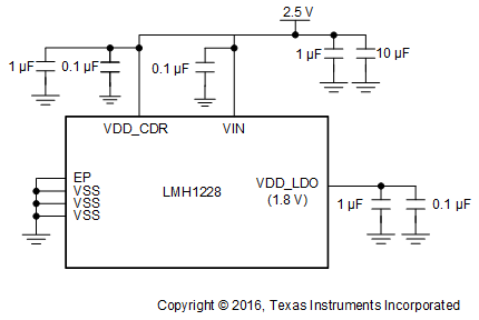
LMH1228 power_supply_recommendation_lmh1228_snls575.gifFigure 41. Recommended Power Supply Decoupling

Good supply bypassing requires low inductance capacitors. This can be achieved through an array of multiple small body size surface-mount bypass capacitors to keep low supply impedance. Better results can be achieved through the use of a buried capacitor formed by a VDD and VSS plane separated by 2 to 4 mil dielectric in a printed-circuit board.