JAJSJA6A September 2021 – December 2021 LMH5485-SP
ADVANCE INFORMATION
- 1 特長
- 2 アプリケーション
- 3 概要
- 4 Revision History
- 5 Device Comparison Table
- 6 Pin Configuration and Functions
-
7 Specifications
- 7.1 Absolute Maximum Ratings
- 7.2 ESD Ratings
- 7.3 Recommended Operating Conditions
- 7.4 Thermal Information
- 7.5 Electrical Characteristics: VS+ – VS– = 5 V
- 7.6 Electrical Characteristics: VS+ – VS– = 3 V
- 7.7 Quality Conformance Inspection
- 7.8 Typical Characteristics: 5 V Single Supply
- 7.9 Typical Characteristics: 3 V Single Supply
- 7.10 Typical Characteristics: 3 V to 5 V Supply Range
- 8 Parameter Measurement Information
-
9 Detailed Description
- 9.1 Overview
- 9.2 Functional Block Diagram
- 9.3 Feature Description
- 9.4
Device Functional Modes
- 9.4.1
Operation from Single-Ended Sources to Differential Outputs
- 9.4.1.1 AC-Coupled Signal Path Considerations for Single-Ended Input to Differential Output Conversion
- 9.4.1.2 DC-Coupled Input Signal Path Considerations for Single-Ended to Differential Conversion
- 9.4.1.3 Resistor Design Equations for the Single-Ended to Differential Configuration of the FDA
- 9.4.1.4 Input Impedance for the Single-Ended to Differential FDA Configuration
- 9.4.2 Differential-Input to Differential-Output Operation
- 9.4.1
Operation from Single-Ended Sources to Differential Outputs
- 10Power Supply Recommendations
- 11Layout
- 12Device and Documentation Support
- 13Mechanical, Packaging, and Orderable Information
パッケージ・オプション
デバイスごとのパッケージ図は、PDF版データシートをご参照ください。
メカニカル・データ(パッケージ|ピン)
- HKX|8
サーマルパッド・メカニカル・データ
発注情報
9.4.1.4 Input Impedance for the Single-Ended to Differential FDA Configuration
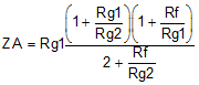
The designs so far have included a source impedance, Rs, that must be matched by Rt and Rg1. The total impedance at the junction of Rt and Rg1 for the circuit of Figure 8-3 is the parallel combination of Rt to ground, and the ZA (active impedance) presented by Rg1. The expression for ZA, assuming Rg2 is set to obtain the differential divider balance, is given by Equation 5:
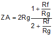
For designs that do not need impedance matching, but instead come from the low impedance output of another amplifier for instance, Rg1 = Rg2 is the single-to-differential design used without an Rt to ground. Setting Rg1 = Rg2 = Rg in Equation 5 gives the input impedance of a simple input FDA driving from a low-impedance, single-ended source to a differential output as shown in Equation 6:
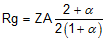
In this case, setting a target gain as Rf / Rg ≡ α, and then setting the desired input impedance, allows the Rg element to be resolved first, and then the required Rf to get the gain. For example, targeting an input impedance of 200 Ω with a gain of 4 V/V, Equation 7 gives the physical Rg element. Multiplying this required Rg value by a gain of 4 gives the Rf value and the design of Figure 9-1.
After being designed, this circuit can also be AC-coupled by adding blocking caps in series with the two 120 Ω Rg resistors. This active input impedance has the advantage of increasing the apparent load to the prior stage using lower resistors values, leading to lower output noise for a given gain target.