SNLS634 June   2020 LMH9126

PRODUCTION DATA.  

  1. Features
  2. Applications
  3. Description
    1.     Device Images
      1.      LMH9126: Differential to Single-Ended Amplifier
  4. Revision History
  5. Pin Configuration and Functions
    1.     Pin Functions
  6. Specifications
    1. 6.1 Absolute Maximum Ratings
    2. 6.2 ESD Ratings
    3. 6.3 Recommended Operating Conditions
    4. 6.4 Thermal Information
    5. 6.5 Electrical Characteristics
    6. 6.6 Typical Characteristics
  7. Detailed Description
    1. 7.1 Overview
    2. 7.2 Functional Block Diagram
    3. 7.3 Feature Description
    4. 7.4 Device Functional Modes
  8. Application and Implementation
    1. 8.1 Application Information
    2. 8.2 Typical Application
      1. 8.2.1 Design Requirements
      2. 8.2.2 Detailed Design Procedure
      3. 8.2.3 Application Curves
  9. Power Supply Recommendations
  10. 10Layout
    1. 10.1 Layout Guidelines
    2. 10.2 Layout Example
  11. 11Device and Documentation Support
    1. 11.1 Documentation Support
      1. 11.1.1 Related Documentation
    2. 11.2 Receiving Notification of Documentation Updates
    3. 11.3 Support Resources
    4. 11.4 Trademarks
    5. 11.5 Electrostatic Discharge Caution
    6. 11.6 Glossary
  12. 12Mechanical, Packaging, and Orderable Information

パッケージ・オプション

メカニカル・データ(パッケージ|ピン)
サーマルパッド・メカニカル・データ
発注情報

Typical Characteristics

at TA = 25°C, VDD = 3.3 V, differential input impedance (ZIN) = 100 Ω, single-ended output impedance (ZLOAD) = 50 Ω, and POUT(TOTAL) = 8 dBm into ZLOAD = 50 Ω (unless otherwise noted)
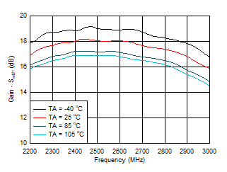
LMH9126 D001gaintempJUN.gif
POUT = 2 dBm
Figure 1. Gain vs Frequency and Temperature
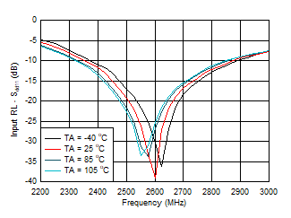
LMH9126 D003S11Temp_JUN.gif
Figure 3. Input Return Loss vs Frequency
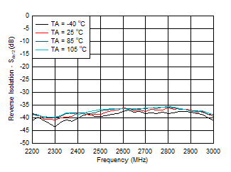
LMH9126 D005S12Temp_JUN.gif
Figure 5. Reverse Isolation vs Frequency
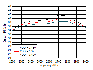
LMH9126 D007OIP3VDD_JUN.gif
POUT/TONE = 2 dBm, 10-MHz tone spacing
Figure 7. Output IP3 vs Frequency and Supply Voltage
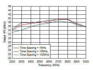
LMH9126 D009OIP3_df_JUN.gif
POUT/TONE = 2 dBm
Figure 9. Output IP3 vs Frequency and Tone Spacing
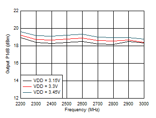
LMH9126 D011P1dB_VDD_JUN.gif
Figure 11. Output P1dB vs Frequency and Supply Voltage
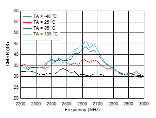
LMH9126 D013CMRR_temp_JUN.gif
Figure 13. CMRR vs Frequency
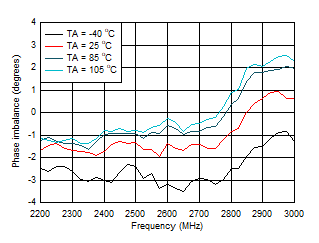
LMH9126 D015Ph_imb_temp_JUN.gif
Figure 15. Phase Imbalance vs Frequency and Temperature
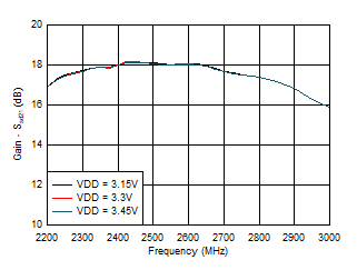
LMH9126 D002gainVDD_JUN.gif
POUT = 2 dBm
Figure 2. Gain vs Frequency and Supply Voltage
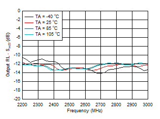
LMH9126 D004S22Temp_JUN.gif
Figure 4. Output Return Loss vs Frequency
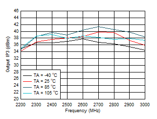
LMH9126 D006OIP3Temp_JUN.gif
POUT/TONE = 2 dBm, 10-MHz tone spacing
Figure 6. Output IP3 vs Frequency and Temperature
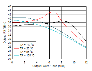
LMH9126 D008OIP3PoutTemp_JUN.gif
f = 2.6 GHz, 10-MHz tone spacing
Figure 8. Output IP3 vs Output Power per Tone
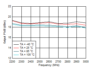
LMH9126 D010P1dB_temp_JUN.gif
Figure 10. Output P1dB vs Frequency and Temperature
LMH9126 D012NF_temp_JUN.gif
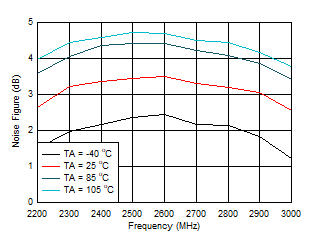
ZSOURCE = 100-Ω differential
Figure 12. Noise Figure vs Frequency and Temperature
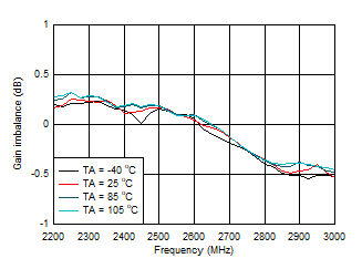
LMH9126 D014_G_imb_temp_JUN.gif
Figure 14. Gain Imbalance vs Frequency and Temperature