JAJSGV2D January 2012 – September 2021 LMK01801
PRODUCTION DATA
- 1 特長
- 2 アプリケーション
- 3 概要
- 4 Revision History
- 5 Device Comparison
- 6 Pin Configuration and Functions
- 7 Specifications
- 8 Parameter Measurement Information
-
9 Detailed Description
- 9.1 Overview
- 9.2 Functional Block Diagram
- 9.3
Feature Description
- 9.3.1 High-Speed Clock Inputs (CLKin0/CLKin0* and CLKin1/CLKin1*)
- 9.3.2 Clock Distribution
- 9.3.3 Small Divider (1 to 8)
- 9.3.4 Large Divider (1 to 1045)
- 9.3.5 CLKout Analog Delay
- 9.3.6 CLKout0 to CLKout11 Digital Delay
- 9.3.7 CLKout12 and CLKout13 Digital Delay
- 9.3.8 Programmable Outputs
- 9.3.9 Clock Output Synchronization
- 9.3.10 Default Clock Outputs
- 9.4 Device Functional Modes
- 9.5 Programming
- 9.6 Register Map
- 10Application and Implementation
- 11Power Supply Recommendations
- 12Layout
- 13Device and Documentation Support
- 14Mechanical, Packaging, and Orderable Information
パッケージ・オプション
メカニカル・データ(パッケージ|ピン)
- RHS|48
サーマルパッド・メカニカル・データ
- RHS|48
発注情報
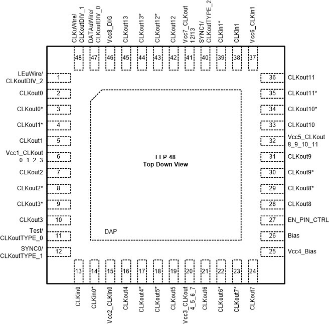
6 Pin Configuration and Functions
 Figure 6-1 48-Pin
Package
Figure 6-1 48-Pin
PackageTable 6-1 Pin Functions(1)
| Pin Number | Name(s) | I/O | Type | Description |
|---|---|---|---|---|
| 1 | LEuWire/ CLKoutDIV_2 |
I | CMOS / 3-State | MICROWIRE Latch Enable Input / Pin control mode: clock divider 2 |
| 2, 3 | CLKout0, CLKout0* |
O | Programmable | Clock output 0: LVDS or LVPECL |
| 4, 5 | CLKout1*, CLKout1 |
O | Programmable | Clock output 1: LVDS or LVPECL |
| 6 | Vcc1_CLKout 0_1_2_3 |
I | PWR | Power supply for clock outputs 0, 1, 2, and 3 |
| 7, 8 | CLKout2, CLKout2* |
O | Programmable | Clock output 2: LVDS or LVPECL |
| 9, 10 | CLKout3*, CLKout3 |
O | Programmable | Clock output 3: LVDS or LVPECL |
| 11 | Test/ CLKoutTYPE_0 |
I/O | CMOS / 3-State | Reserved Test Pin / Pin control mode: clock output type select 0 |
| 12 | SYNC0/ CLKoutTYPE_1 |
I | CMOS / 3-State | SYNC0 / Pin control mode: clock output type select 1 |
| 13, 14 | CLKin0, CLKin0* |
I | ANLG | Clock input 0. Supports clocking types including but not limited to LVDS, LVPECL, and LVCMOS |
| 15 | Vcc2_CLKin0 | I | PWR | Power supply for clock input 0 |
| 16, 17 | CLKout4, CLKout4* |
O | Programmable | Clock output 4: LVDS, LVPECL, or LVCMOS |
| 18, 19 | CLKout5*, CLKout5 |
O | Programmable | Clock output 5: LVDS, LVPECL, or LVCMOS |
| 20 | Vcc3_CLKout 4_5_6_7 |
I | PWR | Power supply for clock outputs 4, 5, 6, and 7 |
| 21, 22 | CLKout6, CLKout6* |
O | Programmable | Clock output 6: LVDS, LVPECL, or LVCMOS |
| 23, 24 | CLKout7*, CLKout7 |
O | Programmable | Clock output 7: LVDS, LVPECL, or LVCMOS |
| 25 | Vcc4_Bias | I | PWR | Power supply for Bias |
| 26 | Bias | ANLG | Bias bypass pin | |
| 27 | EN_PIN_CTRL | I | 3-State | Select MICROWIRE or pin control mode |
| 28, 29 | CLKout8, CLKout8* |
O | Programmable | Clock output 8: LVDS, LVPECL, or LVCMOS |
| 30, 31 | CLKout9*, CLKout9 |
O | Programmable | Clock output 9: LVDS, LVPECL, or LVCMOS |
| 32 | Vcc5_CLKout 8_9_10_11 |
I | PWR | Power supply for clock outputs 8, 9, 10, and 11 |
| 33, 34 | CLKout10, CLKout10* |
O | Programmable | Clock output 10: LVDS, LVPECL, or LVCMOS |
| 35, 36 | CLKout11*, CLKout11 |
O | Programmable | Clock output 11: LVDS, LVPECL, or LVCMOS |
| 37 | Vcc6_CLKin1 | I | PWR | Power supply for clock input 1 |
| 38, 39 | CLKin1, CLKin1* |
I | ANLG | Clock input 1. Supports clocking types including but not limited to LVDS, LVPECL, and LVCMOS |
| 40 | SYNC1/ CLKoutTYPE_2 |
I | CMOS / 3-State | SYNC pin for CLKin1 and bank B. Pin control mode: Clock output type select 2 |
| 41 | Vcc7_CLKout 12_13 |
I | PWR | Power supply for clock outputs 12, and 13 |
| 42, 43 | CLKout12, CLKout12* |
O | Programmable | Clock output 12: LVDS, LVPECL, or LVCMOS |
| 44, 45 | CLKout13*, CLKout13 |
O | Programmable | Clock output 13: LVDS, LVPECL, or LVCMOS |
| 46 | Vcc8_DIG | I | PWR | Power supply for digital |
| 47 | DATAuWire/ CLKoutDIV_0 |
I | CMOS / 3-State | MICROWIRE DATA Pin / Pin control mode: Clock divider 0 |
| 48 | CLKuWire/ CLKoutDIV_1 |
I | CMOS / 3-State | MICROWIRE CLK Pin / Pin control mode: Clock divider 1 |
| DAP | DAP | GND | DIE ATTACH PAD, connect to GND |
(1) See Section 12.1.1 for recommended connections.