SNAS506I January 2011 – December 2014 LMP91000
PRODUCTION DATA.
- 1 Features
- 2 Applications
- 3 Description
- 4 Revision History
- 5 Pin Configuration and Functions
- 6 Specifications
-
7 Detailed Description
- 7.1 Overview
- 7.2 Functional Block Diagram
- 7.3 Feature Description
- 7.4 Device Functional Modes
- 7.5 Programming
- 7.6 Registers Maps
- 8 Application and Implementation
- 9 Power Supply Recommendations
- 10Layout
- 11Device and Documentation Support
- 12Mechanical, Packaging, and Orderable Information
6 Specifications
6.1 Absolute Maximum Ratings
over operating free-air temperature (unless otherwise noted) (1)| MIN | MAX | UNIT | ||
|---|---|---|---|---|
| Voltage between any two pins | 6.0 | V | ||
| Current through VDD or VSS | 50 | mA | ||
| Current sunk and sourced by CE pin | 10 | mA | ||
| Current out of other pins(2) | 5 | mA | ||
| Junction Temperature (3) | 150 | °C | ||
| Storage temperature | –65 | 150 | °C | |
(1) Stresses beyond those listed under Absolute Maximum Ratings may cause permanent damage to the device. These are stress ratings only, which do not imply functional operation of the device at these or any other conditions beyond those indicated under Recommended Operating Conditions. Exposure to absolute-maximum-rated conditions for extended periods may affect device reliability.
(2) All non-power pins of this device are protected against ESD by snapback devices. Voltage at such pins will rise beyond absmax if current is forced into pin.
(3) The maximum power dissipation is a function of TJ(MAX), RθJA, and the ambient temperature, TA. The maximum allowable power dissipation at any ambient temperature is PDMAX = (TJ(MAX) - TA)/ θJA All numbers apply for packages soldered directly onto a PCB.
6.2 ESD Ratings
| VALUE | UNIT | |||
|---|---|---|---|---|
| V(ESD) | Electrostatic discharge | Human-body model (HBM), per ANSI/ESDA/JEDEC JS-001(1) | ±2000 | V |
| Charged-device model (CDM), per JEDEC specification JESD22-C101(2) | ±1000 | |||
(1) JEDEC document JEP155 states that 500-V HBM allows safe manufacturing with a standard ESD control process.
(2) JEDEC document JEP157 states that 250-V CDM allows safe manufacturing with a standard ESD control process.
6.3 Recommended Operating Conditions
| MIX | MAX | UNIT | |||
|---|---|---|---|---|---|
| Supply Voltage VS= (VDD - AGND) | 2.7 | 5.25 | V | ||
| Temperature Range(1) | –40 | 85 | °C | ||
(1) The maximum power dissipation is a function of TJ(MAX), RθJA, and the ambient temperature, TA. The maximum allowable power dissipation at any ambient temperature is PDMAX = (TJ(MAX) - TA)/ θJA All numbers apply for packages soldered directly onto a PCB.
6.4 Thermal Information
| THERMAL METRIC(1) | LMP91000 | UNIT | |
|---|---|---|---|
| WSON | |||
| 14 PINS | |||
| RθJA | Package Thermal Resistance | 44 | °C/W |
(1) For more information about traditional and new thermal metrics, see the IC Package Thermal Metrics application report, SPRA953.
6.5 Electrical Characteristics
Unless otherwise specified, TA = 25°C, VS=(VDD – AGND), VS = 3.3 V and AGND = DGND = 0 V, VREF = 2.5 V, Internal Zero = 20% VREF.(1)| PARAMETER | TEST CONDITIONS | MIN(3) | TYP(2) | MAX(3) | UNIT | ||
|---|---|---|---|---|---|---|---|
| POWER SUPPLY SPECIFICATION | |||||||
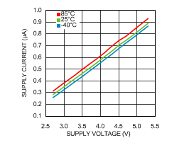
| IS | Supply Current | 3-lead amperometric cell mode | µA | ||||
| MODECN = 0x03 | 10 | 13.5 | |||||
| –40 to 80°C (please verify that the degree is correct) | 15 | ||||||
| Standby mode | |||||||
| MODECN = 0x02 | 6.5 | 8 | |||||
| –40 to 80°C | 10 | ||||||
| Temperature Measurement mode with TIA OFF | |||||||
| MODECN = 0x06 | 11.4 | 13.5 | |||||
| –40 to 80°C | 15 | ||||||
| Temperature Measurement mode with TIA ON | |||||||
| MODECN = 0x07 | 14.9 | 18 | |||||
| –40 to 80°C | 20 | ||||||
| 2-lead ground-referred galvanic cell mode | |||||||
| VREF=1.5 V | 6.2 | ||||||
| MODECN = 0x01 | 8 | ||||||
| –40 to 80°C | 9 | ||||||
| Deep Sleep mode | |||||||
| MODECN = 0x00 | 0.6 | 0.85 | |||||
| –40 to 80°C | 1 | ||||||
| POTENTIOSTAT | |||||||
| Bias_RW | Bias Programming range (differential voltage between RE pin and WE pin) | Percentage of voltage referred to VREF or VDD | ±24% | ||||
| Bias Programming Resolution | First two smallest step | ±1 | |||||
| All other steps | ±2% | ||||||
| IRE | Input bias current at RE pin | VDD = 2.7 V | pA | ||||
| Internal Zero 50% VDD | –90 | 90 | |||||
| –40 to 80°C | –800 | 800 | |||||
| VDD = 5.25 V | |||||||
| Internal Zero 50% VDD | –90 | 90 | |||||
| –40 to 80°C | –900 | 900 | |||||
| ICE | Minimum operating current capability | sink | 750 | µA | |||
| source | 750 | ||||||
| Minimum charging capability(5) | sink | 10 | mA | ||||
| source | 10 | ||||||
| AOL_A1 | Open-loop voltage gain of control loop op amp (A1) | 300 mV ≤ VCE ≤ Vs-300 mV; | dB | ||||
| –750 µA ≤ICE ≤ 750 µA | |||||||
| –40 to 80°C | 104 | 120 | |||||
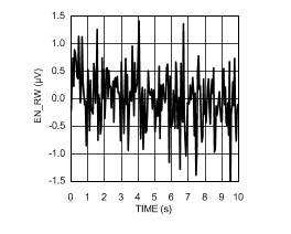
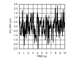
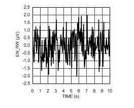
| en_RW | Low Frequency integrated noise between RE pin and WE pin | 0.1 Hz to 10 Hz, Zero Bias (6) |
3.4 | µVpp | |||
| 0.1 Hz to 10 Hz, with Bias (6)(7) |
5.1 | ||||||
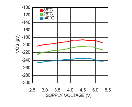
| VOS_RW | WE Voltage Offset referred to RE | BIAS polarity (8) –40 to 80°C |
0% VREF Internal Zero=20% VREF |
–550 | 550 | µV | |
| 0% VREF Internal Zero=50% VREF |
|||||||
| 0% VREF Internal Zero=67% VREF |
|||||||
| ±1% VREF | –575 | 575 | |||||
| ±2% VREF | –610 | 610 | |||||
| ±4% VREF | –750 | 750 | |||||
| ±6% VREF | –840 | 840 | |||||
| ±8% VREF | –930 | 930 | |||||
| ±10% VREF | –1090 | 1090 | |||||
| ±12% VREF | –1235 | 1235 | |||||
| ±14% VREF | –1430 | 1430 | |||||
| ±16% VREF | –1510 | 1510 | |||||
| ±18% VREF | –1575 | 1575 | |||||
| ±20% VREF | –1650 | 1650 | |||||
| ±22% VREF | –1700 | 1700 | |||||
| ±24% VREF | –1750 | 1750 | |||||
| TcVOS_RW | WE Voltage Offset Drift referred to RE from –40°C to 85°C (4) |
BIAS polarity (8) |
0% VREF Internal Zero=20% VREF |
–4 | 4 | µV/°C | |
| 0% VREF Internal Zero=50% VREF |
|||||||
| 0% VREF Internal Zero=67% VREF |
|||||||
| ±1% VREF | –4 | 4 | |||||
| ±2% VREF | –4 | 4 | |||||
| ±4% VREF | –5 | 5 | |||||
| ±6% VREF | –5 | 5 | |||||
| ±8% VREF | –5 | 5 | |||||
| ±10% VREF | –6 | 6 | |||||
| ±12% VREF | –6 | 6 | |||||
| ±14% VREF | –7 | 7 | |||||
| ±16% VREF | –7 | 7 | |||||
| ±18% VREF | –8 | 8 | |||||
| ±20% VREF | –8 | 8 | |||||
| ±22% VREF | –8 | 8 | |||||
| ±24% VREF | –8 | 8 | |||||
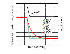
| TIA_GAIN | Transimpedance gain accuracy | 5% | |||||
| Linearity | ±0.05% | ||||||
| Programmable TIA Gains | 7 programmable gain resistors | 2.75 3.5 7 14 35 120 350 |
kΩ | ||||
| Maximum external gain resistor | 350 | ||||||
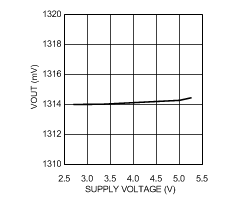
| TIA_ZV | Internal zero voltage | 3 programmable percentages of VREF | 20% 50% 67% |
||||
| 3 programmable percentages of VDD | 20% 50% 67% |
||||||
| Internal zero voltage Accuracy | ±0.04% | ||||||
| RL | Programmable Load | 4 programmable resistive loads | 10 33 50 100 |
Ω | |||
| Load accuracy | 5% | ||||||
| PSRR | Power Supply Rejection Ratio at RE pin | 2.7 V ≤ VDD≤ 5.25 V | Internal zero 20% VREF | 80 | 110 | dB | |
| Internal zero 50% VREF | |||||||
| Internal zero 67% VREF | |||||||
| TEMPERATURE SENSOR SPECIFICATION (Refer to Table 1 in the Feature Description for details) | |||||||
| Temperature Error | TA= –40˚C to 85˚C | –3 | 3 | °C | |||
| Sensitivity | TA= –40˚C to 85˚C | -8.2 | mV/°C | ||||
| Power on time | 1.9 | ms | |||||
| EXTERNAL REFERENCE SPECIFICATION | |||||||
| VREF | External Voltage reference range | 1.5 | VDD | V | |||
| Input impedance | 10 | MΩ | |||||
(1) Electrical Table values apply only for factory testing conditions at the temperature indicated. Factory testing conditions result in very limited self-heating of the device such that TJ = TA.
(2) Typical values represent the most likely parametric norm as determined at the time of characterization. Actual typical values may vary over time and will also depend on the application and configuration. The typical values are not tested and are not specified on shipped production material.
(3) Limits are 100% production tested at 25°C. Limits over the operating temperature range are specified through correlations using statistical quality control (SQC) method.
(4) Offset voltage temperature drift is determined by dividing the change in VOS at the temperature extremes by the total temperature change. Starting from the measured voltage offset at temperature T1 (VOS_RW(T1)), the voltage offset at temperature T2 (VOS_RW(T2)) is calculated according the following formula: VOS_RW(T2)=VOS_RW(T1)+ABS(T2–T1)* TcVOS_RW.
(5) At such currents no accuracy of the output voltage can be expected.
(6) This parameter includes both A1 and TIA's noise contribution.
(7) In case of external reference connected, the noise of the reference has to be added.
(8) For negative bias polarity the Internal Zero is set at 67% VREF.
6.6 I2C Interface
Unless otherwise specified, TA = 25°C, VS = (VDD – AGND), 2.7 V <VS< 5.25 V and AGND = DGND = 0 V, VREF = 2.5 V.(1)| PARAMETER | TEST CONDITIONS | MIN (3) | TYP (2) | MAX(3) | UNIT | ||
|---|---|---|---|---|---|---|---|
| VIH | Input High Voltage |
–40 to 80°C |
0.7*VDD | V | |||
| VIL | Input Low Voltage |
–40 to 80°C |
0.3*VDD | V | |||
| VOL | Output Low Voltage | IOUT= 3 mA | 0.4 | V | |||
| Hysteresis (4) |
–40 to 80°C |
0.1*VDD | V | ||||
| CIN | Input Capacitance on all digital pins |
–40 to 80°C |
0.5 | pF | |||
(1) Electrical Table values apply only for factory testing conditions at the temperature indicated. Factory testing conditions result in very limited self-heating of the device such that TJ = TA.
(2) Typical values represent the most likely parametric norm as determined at the time of characterization. Actual typical values may vary over time and will also depend on the application and configuration. The typical values are not tested and are not specified on shipped production material.
(3) Limits are 100% production tested at 25°C. Limits over the operating temperature range are specified through correlations using statistical quality control (SQC) method.
(4) This parameter is specified by design or characterization.
6.7 Timing Requirements
Unless otherwise specified, TA = 25°C, VS= (VDD – AGND), VS= 3.3 V and AGND = DGND = 0 V, VREF = 2.5 V, Internal Zero= 20% VREF.(1)| MIN | TYP | MAX | UNIT | ||||
|---|---|---|---|---|---|---|---|
| fSCL | Clock Frequency | –40 to 80°C | 10 | 100 | kHz | ||
| tLOW | Clock Low Time | –40 to 80°C | 4.7 | µs | |||
| tHIGH | Clock High Time | –40 to 80°C | 4.0 | µs | |||
| tHD;STA | Data valid | After this period, the first clock pulse is generated | 4.0 | µs | |||
| tSU;STA | Set-up time for a repeated START condition | –40 to 80°C | 4.7 | µs | |||
| tHD;DAT | Data hold time(2)
|
–40 to 80°C | 0 | ns | |||
| tSU;DAT | Data Set-up time | –40 to 80°C | 250 | ns | |||
| tf | SDA fall time (3) | IL ≤ 3 mA; CL ≤ 400 pF –40 to 80°C |
250 | ns | |||
| tSU;STO | Set-up time for STOP condition | –40 to 80°C | 4.0 | µs | |||
| tBUF | Bus free time between a STOP and START condition | –40 to 80°C | 4.7 | µs | |||
| tVD;DAT | Data valid time | –40 to 80°C | 3.45 | µs | |||
| tVD;ACK | Data valid acknowledge time | –40 to 80°C | 3.45 | µs | |||
| tSP | Pulse width of spikes that must be suppressed by the input filter(3) | –40 to 80°C | 50 | ns | |||
| t_timeout | SCL and SDA Timeout | –40 to 80°C | 25 | 100 | ms | ||
| tEN;START | I2C Interface Enabling | –40 to 80°C | 600 | ns | |||
| tEN;STOP | I2C Interface Disabling | –40 to 80°C | 600 | ns | |||
| tEN;HIGH | Time between consecutive I2C interface enabling and disabling | –40 to 80°C | 600 | ns | |||
(1) Electrical Table values apply only for factory testing conditions at the temperature indicated. Factory testing conditions result in very limited self-heating of the device such that TJ = TA.
(2) LMP91000 provides an internal 300-ns minimum hold time to bridge the undefined region of the falling edge of SCL.
(3) This parameter is specified by design or characterization.
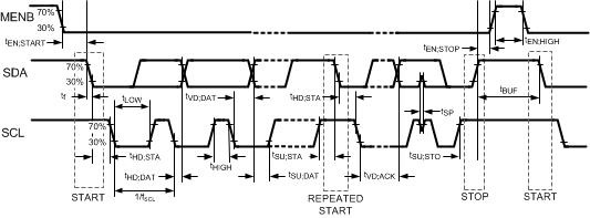
Figure 1. Timing Diagram
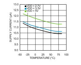
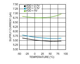
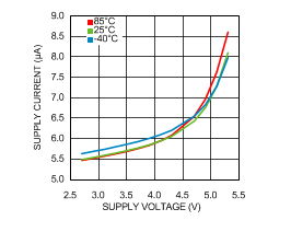
6.8 Typical Characteristics
Unless otherwise specified, TA = 25°C, VS= (VDD – AGND), 2.7V <VS< 5.25 V and AGND = DGND = 0 V, VREF = 2.5 V.
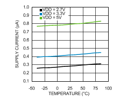
(Deep Sleep Mode)
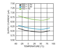
(Standby Mode)
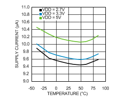
(3-Lead Amperometric Mode)
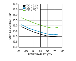
(Temp Measurement TIA On)
(Temp Measurement TIA Off)
(2-Lead Ground-Referred Amperometric Mode)
(Temperature = 30°C)
(Deep Sleep Mode)
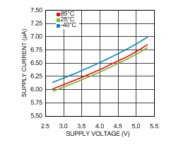
(Standby Mode)
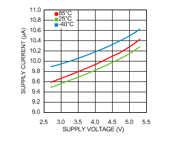
(3-Lead Amperometric Mode)
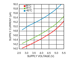
(Temp Measurement TIA On)
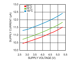
(Temp Measurement TIA Off)
(2-Lead Ground-Referred Amperometric Mode)
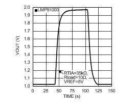
(CO Gas Sensor Connected to LMP91000)