JAJSHB8A May   2019  – October 2019 LMR34206-Q1

PRODUCTION DATA.  

  1. 特長
  2. アプリケーション
  3. 概要
    1.     Device Images
      1. 3.1 概略回路図
  4. 改訂履歴
  5. 概要(続き)
  6. Device Comparison Table
  7. Pin Configuration and Functions
    1.     Pin Functions
  8. Specifications
    1. 8.1 Absolute Maximum Ratings
    2. 8.2 ESD Ratings
    3. 8.3 Recommended Operating Conditions
    4. 8.4 Thermal Information
    5. 8.5 Electrical Characteristics
    6. 8.6 Timing Requirements
    7. 8.7 System Characteristics
    8. 8.8 Typical Characteristics
  9. Detailed Description
    1. 9.1 Overview
    2. 9.2 Functional Block Diagram
    3. 9.3 Feature Description
      1. 9.3.1 Power-Good Flag Output
      2. 9.3.2 Enable and Start-up
      3. 9.3.3 Current Limit and Short Circuit
      4. 9.3.4 Undervoltage Lockout and Thermal Shutdown
    4. 9.4 Device Functional Modes
      1. 9.4.1 Auto Mode
      2. 9.4.2 Forced PWM Operation
      3. 9.4.3 Dropout
      4. 9.4.4 Minimum Switch On-Time
      5. 9.4.5 Spread Spectrum Operation
  10. 10Application and Implementation
    1. 10.1 Application Information
    2. 10.2 Typical Application
      1. 10.2.1 Design Requirements
        1. 10.2.1.1 Design Requirements
      2. 10.2.2 Detailed Design Procedure
        1. 10.2.2.1 Choosing the Switching Frequency
        2. 10.2.2.2 Setting the Output Voltage
        3. 10.2.2.3 Inductor Selection
        4. 10.2.2.4 Output Capacitor Selection
        5. 10.2.2.5 Input Capacitor Selection
        6. 10.2.2.6 CBOOT
        7. 10.2.2.7 VCC
        8. 10.2.2.8 External UVLO
        9. 10.2.2.9 Maximum Ambient Temperature
      3. 10.2.3 Application Curves
  11. 11Power Supply Recommendations
  12. 12Layout
    1. 12.1 Layout Guidelines
      1. 12.1.1 Ground and Thermal Considerations
    2. 12.2 Layout Example
  13. 13デバイスおよびドキュメントのサポート
    1. 13.1 デバイス・サポート
      1. 13.1.1 開発サポート
    2. 13.2 ドキュメントのサポート
      1. 13.2.1 関連資料
    3. 13.3 ドキュメントの更新通知を受け取る方法
    4. 13.4 サポート・リソース
    5. 13.5 商標
    6. 13.6 静電気放電に関する注意事項
    7. 13.7 Glossary
  14. 14メカニカル、パッケージ、および注文情報

パッケージ・オプション

メカニカル・データ(パッケージ|ピン)
サーマルパッド・メカニカル・データ
発注情報

Typical Application

Figure 18 shows for the LMR34206-Q1. This device is designed to function over a wide range of external components and system parameters. However, the internal compensation is optimized for a certain range of external inductance and output capacitance. As a quick start guide, Table 3 provides typical component values for a range of the most common output voltages.
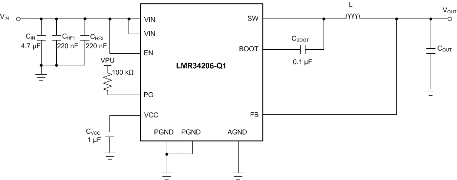
LMR34206-Q1 general_apps_circuit_4206q1-fixed-output.gifFigure 18. Example Applications Circuit (Fixed Output)

Table 3. Typical External Component Values

ƒSW (kHz) VOUT (V) L (µH) Nominal COUT (rated capacitance) (1) Minimum COUT (rated capacitance) (2) CIN
2100 3.3 6.8 2 × 15 µF 1 × 15 µF 4.7 µF + 2 × 220 nF
2100 5 10 2 × 15 µF 1 × 15 µF 4.7 µF + 2 × 220 nF
Optimized for superior load transient performance from 0 to 100% rated load.
Optimized for size constrained end applications.