JAJSHZ4A September 2019 – February 2020 LMR36520
PRODUCTION DATA.
- 1 特長
- 2 アプリケーション
- 3 概要
- 4 改訂履歴
- 5 Description
- 6 Device Comparison Table
- 7 Pin Configuration and Functions
- 8 Specifications
- 9 Detailed Description
-
10Application and Implementation
- 10.1 Application Information
- 10.2
Typical Application
- 10.2.1
Design 1: Low Power 24-V, 2-A Buck Converter
- 10.2.1.1 Design Requirements
- 10.2.1.2
Detailed Design Procedure
- 10.2.1.2.1 Choosing the Switching Frequency
- 10.2.1.2.2 Setting the Output Voltage
- 10.2.1.2.3 Inductor Selection
- 10.2.1.2.4 Output Capacitor Selection
- 10.2.1.2.5 Input Capacitor Selection
- 10.2.1.2.6 CBOOT
- 10.2.1.2.7 VCC
- 10.2.1.2.8 CFF Selection
- 10.2.1.2.9 External UVLO
- 10.2.1.2.10 Maximum Ambient Temperature
- 10.2.2 Application Curves
- 10.2.1
Design 1: Low Power 24-V, 2-A Buck Converter
- 10.3 What to Do and What Not to Do
- 11Power Supply Recommendations
- 12Layout
- 13デバイスおよびドキュメントのサポート
- 14メカニカル、パッケージ、および注文情報
10.2 Typical Application
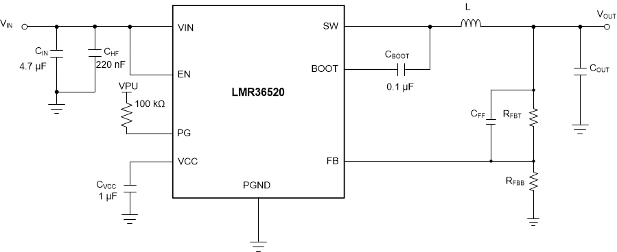
shows a typical application circuit for the LMR36520. This device is designed to function over a wide range of external components and system parameters. However, the internal compensation is optimized for a certain range of external inductance and output capacitance. As a quick-start guide, Figure 13 provides typical component values for a range of the most common output voltages.
 Figure 13. Example Application Circuit
 Table 2. Typical External Component Values
| ƒSW (kHz) | VOUT (V) | L (µH) | NOMINAL COUT (RATED CAPACITANCE) (1) | MINIMUM COUT (RATED CAPACITANCE) (2) | RFBT (Ω) | RFBB (Ω) | CIN | CFF |
|---|---|---|---|---|---|---|---|---|
| 400 | 3.3 | 6.8 | 3 × 22 µF | 3 × 22 µF | 100 k | 43.2 k | 2 × 4.7 µF + 220 nF | None |
| 400 | 5 | 10 | 2 × 22 µF | 2 × 22 µF | 100 k | 24.9 k | 2 × 4.7 µF + 220 nF | None |
| 400 | 12 | 33 | 4 × 10 µF | 4 × 10 µF | 100 k | 9.09 k | 2 × 4.7 µF + 220 nF | None |
(1) Optimized for superior load transient performance from 0 to 100% rated load.
(2) Optimized for size constrained end applications.